Silicon Wafer Processing Educational Research
Get Your Quote FAST!
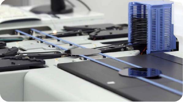
What does a Polished Silicon Wafer Processing Look Like?
Below is what a finsihed silicon wafer after final polish before being added to it's wafer carrier for the next steap. Cleaning.
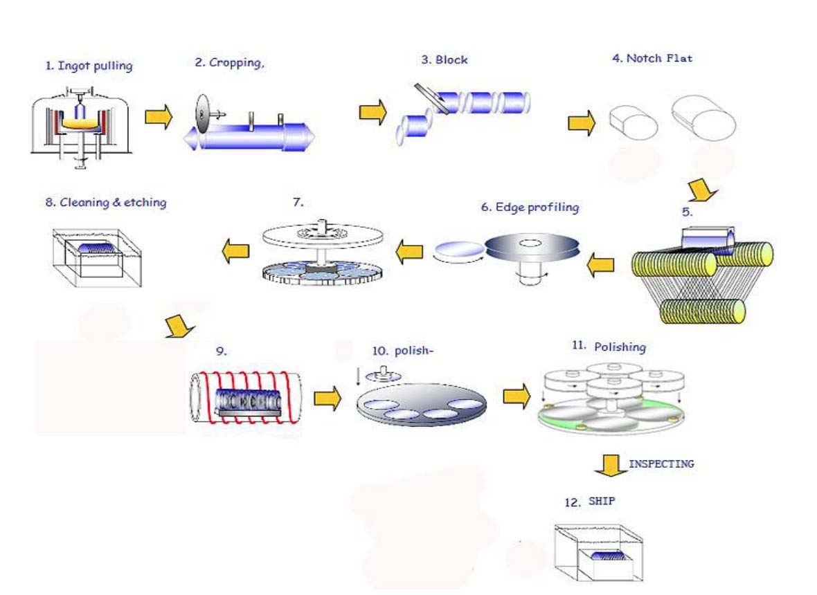
Silicon Wafer Processing Flow Chart
Below is a flow chart for silicon wafer processing from Ingot to device.
What are the Silicon Wafer Process Steps in Order?
- Ingot Pulling
- Cropping
- Block
- Notch Flat
- Edge Profiling
- Cleaning and Etching
- Polishing
- Inspecting
- Shipping
UniversityWafer, Inc. along with our partners provide researchers both university and corporate with the most efficient processing. We delivery on time and under cost.
Please let us know what substrate specificatoins that we can quote for you!