
I need inexpensive 3 inch polished silicon wafers for SU-8 photolithography processing. A thickness of approximately 500 µm is required, and I may need up to 100 wafers for university research.
Silicon Wafers for SU-8 Photolithography
Researchers frequently use silicon wafers for SU-8 photolithography because they provide excellent surface flatness, thermal stability, and compatibility with standard semiconductor processing equipment. Polished silicon wafers are ideal substrates for creating high-resolution SU-8 patterns used in MEMS devices, microfluidic channels, biosensors, and advanced microelectronics.
A graduate student requested the following quote:
Reference #170019 for specifications and pricing.
What is SU-8 Photolithography?
 SU-8 photolithography is a microfabrication process that uses an epoxy-based negative photoresist to create precise microstructures on silicon and glass substrates. During ultraviolet (UV) exposure, the exposed regions become cross-linked and remain after development, allowing researchers to fabricate microchannels, micro-pillars, molds, sensors, and other high-aspect-ratio structures.
Because SU-8 offers excellent chemical resistance, thermal stability, and high-resolution patterning, it is widely used in MEMS fabrication, biomedical devices, lab-on-a-chip systems, optical components, and microfluidic research.
Get Your SU-8 Wafer Quote FAST!
Borofloat 33 Glass Wafers for SU-8 Processing
For applications requiring optical transparency, many researchers choose Borofloat 33 glass wafers as an alternative to silicon substrates. Borofloat glass combines low thermal expansion, excellent optical transmission, and high dimensional stability, making it ideal for microfluidics, optical sensors, and bioanalytical devices.
A PhD candidate requested the following:
We are interested in 100 mm diameter Borofloat 33 glass wafers for SU-8 photolithography and would like to confirm the wafer flat configuration before ordering multiple pieces.
Reference #223367 for specifications and pricing.
Common SU-8 Photolithography Terms
- SU-8 negative photoresist
- UV lithography
- Spin coating
- High aspect ratio structures
- MEMS fabrication
- Microfluidic devices
- Photomask exposure
- Post-exposure bake (PEB)
- Wafer cleaning and preparation
- Semiconductor microfabrication
- Glass and silicon substrates
- Photoresist patterning
- Lab-on-a-chip fabrication
- Biomedical microsystems
SU-8 Photolithography for MEMS and Microfluidic Device Fabrication
SU-8 photolithography is a widely used microfabrication process that employs an epoxy-based negative photoresist to create high-resolution patterns and high-aspect-ratio structures. Because SU-8 can produce thick, mechanically stable features with excellent chemical resistance, it has become a standard material for MEMS fabrication, microfluidics, biosensors, optical devices, and semiconductor research.
Researchers commonly apply SU-8 photoresist to silicon wafers, Borofloat 33 glass wafers, and other substrate materials using a precision spin-coating process. Following soft bake, UV exposure, post-exposure bake, and development, the resulting structures can exhibit aspect ratios exceeding 20:1 depending on processing conditions.
What Makes SU-8 Photoresist Unique?
Unlike positive photoresists, SU-8 is a negative photoresist. Areas exposed to ultraviolet light become cross-linked and remain after development, while unexposed regions are removed. This property enables the fabrication of deep microchannels, micro-pillars, microfluidic molds, and other three-dimensional structures used in advanced research and manufacturing.
Key advantages of SU-8 photoresist include:
- High aspect ratio microstructures
- Excellent chemical resistance
- Strong mechanical stability
- High thermal resistance
- Compatibility with silicon and glass substrates
- Excellent pattern resolution
- Biocompatibility for biomedical applications
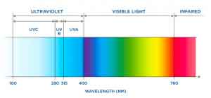
UV Exposure and SU-8 Processing
Successful SU-8 lithography depends on precise ultraviolet exposure, baking conditions, and development times. The photoresist is typically exposed using near-UV wavelengths around 365 nm, which initiate cross-linking within the epoxy matrix. Proper control of exposure dose and post-exposure bake temperature helps prevent cracking, incomplete development, and feature distortion.
Exposure parameters must be optimized based on photoresist thickness, substrate reflectivity, and feature size. Thick SU-8 layers often require higher exposure energies and carefully controlled baking cycles to minimize internal stress.
Applications of SU-8 Photolithography
SU-8 photoresist is used in a wide range of research and commercial applications including:
- Microfluidic device fabrication
- MEMS sensors and actuators
- Lab-on-a-chip platforms
- Biomedical and biosensor devices
- Optical waveguides and photonics
- Micro-molding and replication processes
- Semiconductor packaging and interconnects
- High-aspect-ratio lithography
Choosing the Right Substrate for SU-8 Processing
Both silicon wafers and Borofloat 33 glass wafers are popular substrate choices for SU-8 processing. Silicon provides excellent flatness and compatibility with semiconductor fabrication equipment, while Borofloat glass offers optical transparency and low thermal expansion, making it useful for microfluidic and optical applications.
UniversityWafer supplies silicon wafers, glass wafers, thermal oxide wafers, and custom substrates suitable for SU-8 photolithography, MEMS fabrication, and microfluidic device development.