Substrates Used for Thin Film Solar Panels Fabrication
Get Your Quote FAST!
What is Thin Film Solar Panels?
Thin-film solar panels are a type of photovoltaic cell that uses a thin layer of photovoltaic material, such as amorphous silicon or cadmium telluride, to convert sunlight into electricity. Thin-film solar panels are typically less efficient at converting sunlight into electricity than traditional crystalline silicon solar panels, but they are typically cheaper to produce and can be made in a flexible form, which makes them suitable for use in a variety of applications. Thin-film solar panels are often used in portable electronic devices, such as calculators and satellite-powered devices, as well as in building-integrated photovoltaics, where they can be used as part of the building's exterior.
Indium Tin Oxide Thin Film Solar Panels
Among the various solar panels on the market today, there are many types that are made of indium tin oxide thin film. The main advantage of these panels is their ability to absorb light efficiently. They are also low in resistivity, have high transmittance and can be used in a variety of applications. These characteristics make them ideal for use in solar energy production systems.
Four efficient layers
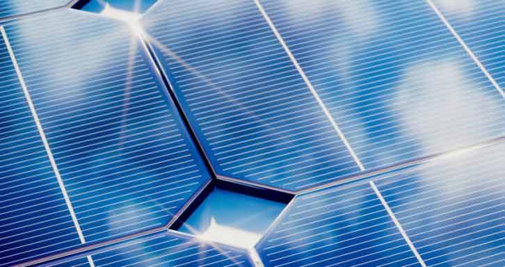
Various types of thin film solar panels are manufactured. Thin film PV technology has evolved into an important branch of sustainable energy production. It has gained popularity in residential and industrial applications.
The market share of thin film solar panels has increased in the last decade. These panels are ideal for BIPV applications. They are flexible and can be installed on a variety of surfaces. They are also lightweight and durable. They are a good alternative to traditional c-Si solar panels. In the future, this technology could expand its market value in the residential and industrial sectors.
Cu2ZnSnSe4 solar cells have recently emerged as a replacement for thin-film PV. These solar cells have excellent optoelectronic properties. However, their conversion efficiency is relatively low. In order to improve the overall performance of these devices, various approaches have been taken. Some of the approaches include replacing the Molybdenum-coated soda lime glass with transparent conducting oxides, introducing a metal grid, and enhancing the charge collecting property of ITO-based DSSCs.
An effective method for improving the current efficiency of the device is to incorporate a p-type oxide semiconductor anode interfacial layer. This can dramatically increase the power conversion efficiency, especially under bifacial illumination. In addition, the OPV interlayer concept should be extended to other p-type materials with an appropriate work function.
This layer can be produced by sputtering or chemical bath deposition. In addition, the thickness of the layer can be controlled to optimize the light-absorbing area. The optimum interlayer thickness is between 5 and 10 nm. It was found that the FF of a 10-nm-thick layer was 37% greater than a 5-nm-thick layer. It also led to a 6% increase in Jsc and a 24% increase in Voc.
Optical bandgap energy
Optical bandgap energy from indium tin oxide thin film solar panels has been investigated. The results indicate that the optical bandgap is significantly enhanced from 3.59 to 4.07 eV with increasing carrier concentration. It is also found that the bandgap energy increases with substrate temperature.
The annealing process also has an effect on the electrical properties of the films. It increases the thickness of the film and induces the crystal structure. It also reduces the resistivity and improves the mobility of the film. In addition, it changes the crystal orientation. The preferred orientation is determined by the amount of crystallite growth along the plane.
The electrical conductivity of the film is related to the bandgap energy. It is calculated using the Davis and Mott model. The bandgap energy is the photon energy at the point (ahv)2 = 0 where a = 0. The n is the index of transition. This is a Planck constant.
The optical transmission of the ITO thin films has been improved from 77% to 88% in the visible region. The increase in transmittance is due to reduced incident light scattering. The annealing and thermal annealing processes have a positive influence on the structural and electrical characteristics of the films. It is also believed that Sn doping reduces the resistivity of the films.
The optical absorption spectrum is one of the most important tools for understanding the band structure. It shows that a decrease in the UV emissions peak is due to the substitution of Sn in the In-O system. This indicates the modification of recombination centers by Sn doping. The blue emission band is caused by the addition of a new defect level. The green emission is attributed to the singly ionized oxygen vacancies.
Low resistivity
Among many types of thin film semiconductors, indium tin oxide (ITO) is one of the most commonly used. Its unique properties as a transparent semiconductor are advantageous for various electronic applications. ITO thin films are particularly useful for electronic devices such as flat panel displays, solar cells, and optical components.
ITO thin films have a high optical transparency of about 95% in the wavelength range of 550-650 nm. The grain size of ITO films is around 7 nm. Its conductive properties are also favorable. ITO has a low resistivity of 10-4 O-cm and a large bandgap of 4 eV. In addition, it can be deposited using radio frequency magnetron sputtering.
During the preparation of ITO films, the effect of substrate temperature on the structure and electrical conductivity was investigated. At a low temperature, ITO films exhibited a polycrystalline structure. However, as the temperature increased, the film exhibited a decreasing resistivity. This was attributed to the interfacial oxide layer. It was thought that the interfacial oxide layer plays an important role in the reduction of the short circuit current density of ITO films.
Moreover, a pure ITO film can replace conventional bus-bar metal electrodes. It has a low resistance and can be used to avoid shadow loss problems. It is also possible to reduce resistance without increasing the thickness of the film. ITO thin films have been applied in various optoelectronic devices, such as organic light emitting diodes, solar cells, and sensors.
ITO has been used as photocathode material in p-type dye-sensitized solar cells. It has a fill-factor of 0.45, which is higher than that of other semiconductors. Its open circuit voltage is 0.55 V.
High transmittance
Optical transmittance of indium tin oxide thin film solar panels was studied. ITO films were deposited on glass substrates by RF magnetron sputtering. The mass ratio of indium to tin was varied to study the effects on light transmittance. In this study, films were found to have greater transmittance as the tin content in the film increased.
An average value of optical transmittance was calculated for a wavelength range of 400-760 nm. The results showed that a higher substrate temperature improved the adhesion of the layer to the substrate. It also increased the mobility and energy of the atoms.
Increasing the mass ratio of indium to tin in the film increased the electrical conductivity. This resulted in lower resistivity values. An ITO-5 film deposited with a MIn/MSn mass ratio of 9.25 exhibited optimal electrical properties. Optical properties were also improved with a further increase in the mass ratio of indium to tin.
Various studies were carried out to determine the influence of the surface roughness on the optical properties of the film. The film exhibited polycrystalline structure when it was exposed to high screen voltages. However, low screen voltage films exhibited amorphous structure. These films had high optical transmittance.
Using a stylus profiler, thickness of the grown coatings was measured. The thickness of the films varied between 755-800 nm. The evaporator was a K type thermocouple and a distance of 0.10 m was maintained between the glass substrates and the evaporator. The current through the evaporator was 75 A.
Transmittance of ITO films was examined for the visible and ultraviolet light spectrum. The results showed that ITO has an optical transparency of 96%. This result was achieved when the film was annealed under appropriate conditions.
Ion bombardment upon the p layer on the performance of the Si HJ solar cell
During the process of deposition of ITO, ion bombardment is a common feature. Several techniques have been used to minimize the impact of ion bombardment. One method is the hot wire chemical vapor deposition (HWCVD) technique. The other is the ion implantation technique.
The latter is an effective technique for adding metal ions to the B-site of perovskites. However, this technique has a downside. It can increase the electrical properties of solar cells, but it can also reduce the stability of the device. This study explores the effects of ion bombardment on the performance of a Si HJ solar cell.
The ion implantation technique was employed to insert Ag ions in place of Pb ions. This ion-implantation approach allowed precise doses and depths. It also facilitated lateral growth and control of doping levels. The process required a low temperature process, which enabled precise doping depths.
Another method of forming p-n junctions in such structures is surface doping. This process entails evaporating Au/Zn/Au (10/30/200 nm) to form a back ohmic contact. This contact increased the wettability of the photo-active layer. It was not, however, optimized for optical performance.
The ion implantation technique has many advantages over other methods. It allows for a precise dose, and it is a more effective method of doping metal ions into the B-site. But, its effects on the performance of a solar cell were not well documented. The present study investigates the influence of ion bombardment on the p layer of a Si HJ solar cell.
One of the most significant effects was the formation of indium-rich clusters during the deposition of ITO. The resulting NPs have anti-reflective properties. The upper edge of the valence band is partly due to the 5s orbitals of Ag. The lower edge is partly due to the 6p empty orbitals of Pb2+.