What is an NMOS Transistor?
If you've been wondering what is an NMOS transistor, then you're not alone. There are a number of other 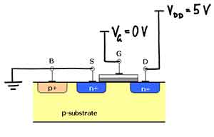 transistors that use this technology, and you may be wondering how they work. Here are some of the basic concepts behind the NMOS transistor. To understand what it is, we need to understand the way that it works. Firstly, the NMOS device works by presenting an ohmic resistance for a fixed VGS.
The NMOS transistor consists of two n-type regions, the source and drain, which are implanted at separate points on the semiconductor. When the gate voltage is positive, electrons are drawn into the channel, which increases conductivity between the source and drain. The opposite is true when the gate voltage is negative, as it cuts off the channel. During this reverse-biased state, an NMOS transistor is said to be ON.
An NMOS transistor is formed by combining a semiconductor crystal substrate made of silicon. This substrate is topped with a thin insulating layer, usually silicon dioxide. A metal or polycrystalline silicon gate is inserted on the top of the semiconductor layer. The crystal region on one side of the gate is called the source. The channel underneath the gate is known as the drain. The NMOS transistor is similar to a conventional NPN transistor in its basic structure.
 The CMOS transistor works by separating the source and drain terminals with a dielectric layer. The gate is separated from the substrate by a dielectric layer. The positive and negative charges attract one another and form a conduction path between the source and drain terminals. The threshold voltage is the lowest voltage needed to form an inversion layer. Once this voltage is reached, the drain-source current is zero.
To understand how an nMOS transistor works, we must understand how pMOS and nMOS transistors work. The pMOS transistor has a gate that conducts when the input is logic 0. On the other hand, the nMOS gate conducts when the input is logic 1, and when the gate is connected to ground, it produces a logical one. This means that an nMOS transistor is a series transistor, and a series transistor implements an inverter.
When designing a computer, you have to consider the type of semiconductor you're using. Ideally, the transistor will be symmetric, so that it operates at the same time in both directions. You can use this to make a faster-performing circuit. There are some benefits of NMOS over PMOS for different purposes. This technology is cheaper and less susceptible to noise. It is also considered faster than PMOS.
In comparison to a conventional NMOS transistor, a PMOS transistor is a semiconductor device that operates in a symmetrical voltage range. It works on the same principle as a NMOS transistor, but is much more complex. Its size is similar to that of an NMOS transistor. The NMOS transistor's gate size, VGS, is essentially a rectangular-shaped ring of alternating current.
Video: N Channel MOSFET Transistor
Why Electrons in NMOS Transistors Don't Travel Further Than Depletion Region
A depletion region is formed by a balance between the diffusion pressure and drift current. As electrons and holes travel from the P-side to the N-side, they combine at the junction, leaving a positive and a negative charge on each side. This opposing force helps determine the width of the depletion region. The amount of charge transfer determines the width of the depletion region.
Transport mechanism of conduction electrons
The transport mechanism of conduction electrons is a general concept and applies to all solids. Without an external magnetic or electrical field, conduction electrons move at the same rate in all directions. They do not transfer charge or spin, but instead move at a constant speed. However, the presence of an electrical field breaks this balance, and the electrons start moving in one direction. Therefore, a transistor can only be switched on when there is sufficient current flowing through it.
In an NMOS transistor, the main current is largely determined by the conduction of electrons. The injected electrons experience multiple e-e scatterings when they reach the T-branch region. They will then transfer their forward momentum to many cold electrons. This is what happens when the voltage in the transistor reaches 0.225 V. In this case, the injected electrons enter the gate region and encounter the transport mechanism of conduction electrons.
In a nano-scaled MOS transistor, the transport mechanism of conduction electrons depends on the phonon bath, MN-scattering, and interface roughness. The phonon-scattering process plays a minor role in low-temperature transport in Si MOS transistors. The phonon-scattering process influences NMOS transistors' ON-state current and limits the drivability of nanotransistors.
An NMOS transistor works by enabling conduction electrons through the crystal lattice. This process is known as ballistic electron conduction and can be exploited to create quantum systems at the nanoscale. By using the quantum mechanical properties of electron wave functions, a semiconductor can use double-slit interference or spatial resonance to create highly efficient electronic systems. For example, it can use the Sharvin resistance, which corresponds to the specific resistivity of two contacting surfaces.
In the previous generation of Si MOS devices, the collector current was small and the ratio between the emitter and collector current was much smaller than unity. This difference in the two devices is caused by the concentration of the channel doping. Previously, the channel was heavily doped with boron, and boron concentration was on the order of 1018 cm-3. Therefore, eliminating impurity scattering is crucial for the present observations.
Charge accumulation/depletion region
The charge accumulation/depletion region of an NMOS transistor is the space in which carriers can accumulate. It is a region of reduced density. The charge density of a hole is 1.6x10⁻¹⁹ coulombs per volume, so that when the hole concentration is high, it will drift along the direction of the electric field. The opposite charge is neutralized by diffusion, so that the holes move in the direction of decreasing density. If the density gradient is positive, then the current flows in the direction of decreasing concentration. If the current is negative, the hole density will be replaced by electron carriers, and this will result in negative current.
The charge on the layer is countered by the presence of mobile electrons at the interface between the semiconductor and gate metal. The presence of this region results in the formation of an inversion layer, which decreases the effective dielectric thickness. This layer is consistent with the presence of a depletion region. As a result, the semiconductor remains in thermal equilibrium when applied to a voltage.
The accumulation/depletion region in an NMOS transistor occurs at a voltage below the threshold voltage. This process is known as depletion, and occurs when a positive charge on the gate pushes a mobile hole into the substrate, leaving the semiconductor with a negative charge. The accumulation/depletion region is separated by a flatband voltage. If the voltage rises to a certain level, the transistor transitions to an inverted state.
The charge accumulation/depletion region of an NMOS transistor is similar to that of an ohmic contact. The gate is shorted to the substrate. This electrically shortens the gate material, resulting in an accumulation/depletion region. The depletion region forms when the gate electrode is at a higher voltage than the flat band voltage. The ohmic gate is the same type of material, with the difference being that the gate is made up of an insulating layer.
The depletion mode MOSFET is the opposite of the enhancement mode. Its channel conducts when the gate-source voltage (VGS) is positive. The channel is normally closed when VGS is negative. The positive gate-source voltage causes the channel to become conductive, and when the gate voltage is negative, the current flows in the drain. The negative gate-source voltage turns the transistor off.
Effective length of mean-free path
The effective length of the mean-free path in NMOS transistors is a measure of the amount of electron scattering in the channel. This parameter is determined by measuring the reflected carrier's kinetic energy and using the band profile. Fig. 2(a) shows the energy profile of a band-emitting transistor. The top-end population of left-moving carriers is large, as the longitudinal field increases. The effective length of the mean-free path at the top of the band is a function of the surface potential and the gate voltage.
The MFP of electrons is defined by a series of equations. One of these equations is the effective length of the channel, which must be less than the mean-free path. For a nanoscale device, the channel length must be much smaller than the effective length of the electrons' mean-free path. It is important to remember that the mean-free path of an electron is extremely energy-dependent. Hence, the resolution of the electron MFP spectrum is essential for understanding the operation of a device and its efficiency.
In a NMOS transistor, there are three basic configurations: first gate 540, second gate 240, and channel 530. The first gate 540 has arms that are near the channel edge and a triangular sawtooth profile. The channel length is less than the electron mean-free path in the channel material. Hence, the second gate is also located near the channel edge.
The long-channel model is the correct one. However, it requires unrealistically low values of L/a and VT for a good fit. The maximum value of L/a is more than 109 in simulation. The maximum length of the channel is 156 O-um. The effective length of the mean-free path in a NMOS transistor is approximately 141 nm.
To construct an NMOS transistor, the effective length of the channel must be smaller than the electron mean-free path. In order to obtain a transistor with the maximum current, the channel must have a length less than the electron mean-free path in the material. Then, the gate voltage restores the shape of the periodic channel. After this process, the voltage drops to zero and the transistor switches from ON to OFF.
Effect of vertical electric field on conduction electrons
Electric fields induce non-equilibrium carrier redistribution, which leads to higher temperature of injected carriers. During conduction, holes and electrons transfer from L valley to k hill, and recombine at the K point. In this way, the voltage drop across the transistor is a function of electric field. This process can be repeated with other types of devices and materials.
The vertical electric field is determined by three factors: the current density, carrier mobility, and the space-charge-limited current model. These three factors determine the vertical electric field in the NMOS transistor. The peak electric field at the pn junction increases with increasing reverse bias, while the peak potential in the hole channel decreases as the carriers diffuse from the surface. The voltage-dependent electric field in NMOS transistors is approximately the same as in other semiconductors, but the vertical electric field is much higher.
A vertically stacked NMOS transistor has a layered structure, as shown in Figure 1e-g. The insulating layer traps electrons, whereas the drain region partially de-traps them from the substrate. These trapped electrons compete for energy with competing lateral fields at the drain and gate. Moreover, the Si-substrate's backside potential has a strong influence on the charge dispersion. Although the dispersion is moderate for a source-biased substrate, it has been found to be excessive in drain-biased structures.

 2"Ø×300±25µm, p-type Si:B[100], Ro=(1-10)Ohmcm,