
"We suddenly have a need for a few 6" silicon wafers. I would like to get 5 pieces. Lot #3175 or Lot #478 would be fine, but we could accept any available lot that can be shipped immediately."
Silicon Wafers for Semiconductor Engineers
Semiconductor engineers rely on high-quality silicon wafers to develop integrated circuits, MEMS devices, sensors, photonic components, power electronics, and advanced semiconductor technologies. Whether working in research laboratories, university cleanrooms, or high-volume fabrication facilities, engineers require substrates with precise specifications, fast delivery, and consistent material quality.
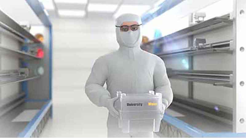
A Senior Semiconductor Engineer Requested:
UniversityWafer Response:
Reference Quote #239225 for specifications, availability, and pricing. We maintain an extensive inventory of silicon substrates, including prime-grade, test-grade, DSP, SSP, SOI, and specialty wafers for semiconductor engineering applications.
Get Your Quote Fast! Or Buy Silicon Wafers Online and start researching today!
How Semiconductor Engineers Use Silicon Wafers
Semiconductor engineers transform silicon wafers into electronic devices through a series of highly controlled fabrication processes. These manufacturing steps are used to create microprocessors, memory devices, sensors, RF components, power semiconductors, and photonic integrated circuits.
-
Wafer Preparation
The wafer surface is cleaned, polished, and inspected to remove contamination and defects before fabrication begins. -
Photolithography
Circuit patterns are transferred onto the wafer using photoresist materials and advanced optical exposure systems. -
Etching
Selective material removal creates the microscopic structures required for semiconductor devices. -
Doping and Ion Implantation
Controlled impurities are introduced into the silicon crystal to create regions with specific electrical properties. -
Thin-Film Deposition
Materials such as oxides, nitrides, polysilicon, and metals are deposited to form device layers and interconnections. -
Wafer Testing and Metrology
Engineers verify device performance, monitor critical dimensions, and optimize manufacturing yield.
Throughout semiconductor fabrication, engineers carefully control temperature, pressure, contamination levels, chemical concentrations, and process parameters to ensure reliable device performance and high production yields.
What Does a Semiconductor Engineer Do?
A semiconductor engineer designs, develops, tests, and improves semiconductor devices used in computers, smartphones, automotive electronics, telecommunications equipment, medical devices, artificial intelligence systems, and advanced research applications. These engineers work with silicon wafers, compound semiconductors, thin films, photolithography equipment, deposition systems, and semiconductor packaging technologies to manufacture integrated circuits and microelectronic devices.
Semiconductor engineers play a critical role throughout the semiconductor manufacturing process, from wafer selection and device design to fabrication, testing, packaging, and yield optimization. Their work helps improve chip performance, reduce power consumption, and increase manufacturing efficiency.
Wafer Specifications Semiconductor Engineers Select
Substrate selection connects the device design to the fabrication process. Engineers specify wafer properties that fit the intended electrical behavior, coating stack, lithography equipment and mechanical requirements.
- Electrical properties: Choose n-type silicon or p-type silicon, dopant and resistivity.
- Geometry: Specify diameter, thickness, crystal orientation, flatness and tolerances.
- Surface finish: Select single-side or double-side polish for the process.
- Layer structure: Use SOI wafers when the design calls for a silicon device layer and buried oxide, or specify thermal oxide coatings separately.
For a material quote, provide the required specification, quantity and application. Request silicon wafers for engineering research.
Types of Semiconductor Engineering Careers
The semiconductor industry offers several engineering career paths, each focused on a different stage of chip development and manufacturing.
Semiconductor Process Engineer
Semiconductor process engineers develop and optimize fabrication processes such as oxidation, diffusion, ion implantation, deposition, CMP, and plasma etching. Their primary goal is improving device performance, yield, and manufacturing efficiency.
Semiconductor Test Engineer
Semiconductor test engineers design and execute electrical testing procedures that verify chip functionality, reliability, and performance. They work with automated test equipment (ATE), wafer probing systems, and statistical process control tools.
IC Design Engineer
Design engineers create integrated circuits, microprocessors, memory devices, RF components, and custom semiconductor solutions using advanced electronic design automation (EDA) software.
Semiconductor Packaging Engineer
Packaging engineers develop methods to protect semiconductor devices while improving electrical performance, thermal management, and long-term reliability.
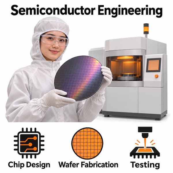
How to Become a Semiconductor Engineer
Electrical and electronics engineering roles typically require at least a bachelor’s degree in a related engineering field, according to the U.S. Bureau of Labor Statistics. Semiconductor job requirements vary by specialization and employer.
- Build a technical foundation: Study mathematics, physics, circuits, electronics and semiconductor device principles.
- Choose a focus: Compare IC design, process development, test engineering and packaging with the type of work you want to do.
- Develop practical experience: Use laboratory classes, projects, internships or research to practice measurement, data analysis and technical documentation.
- Match the job requirements: Review the degree, tools and experience listed for each role. Advanced research positions may call for graduate study.
Skills Used in Semiconductor Engineering
- Device physics and materials: Understand how semiconductor doping, material properties and device structures affect performance.
- Process knowledge: For fabrication roles, learn photolithography, deposition, etching, contamination control and process integration.
- Measurement and analysis: Interpret test results, investigate defects and use data to evaluate process changes.
- Tools suited to the role: Design engineers use EDA tools, while process and test engineers work with fabrication or measurement systems and analysis software.
- Communication: Document experiments, explain results and coordinate with engineers, technicians and manufacturing teams.
Semiconductor Engineer Salary and Career Outlook
Pay depends on job function, experience, location and employer. “Semiconductor engineer” covers several specializations, so a single salary figure can hide substantial differences between roles.
For U.S. salary and employment context, consult the BLS profiles for electrical and electronics engineers and computer hardware engineers. These are broader occupational categories, not salary estimates for every semiconductor job. Compare the survey year, location and job duties when using wage data.
Career settings include semiconductor fabrication facilities, foundries, integrated device manufacturers, fabless chip companies, equipment suppliers, universities and research laboratories. The mix of design, laboratory, cleanroom and production work depends on the position.
Semiconductor Engineering Career Questions
What is the difference between process and test engineering?
A process engineer develops and controls fabrication steps. A test engineer develops measurements and test procedures to evaluate device functionality and performance. Both use data to investigate problems and improve results.
Do all semiconductor engineers work in cleanrooms?
No. Fabrication roles can involve cleanroom work, while design, simulation and some test roles may be based mainly in offices or laboratories.
What specifications should an engineer include in a wafer quote?
Include material, diameter, thickness, crystal orientation, conductivity type, dopant, resistivity, polish, coatings and quantity. Add any tolerances or measurement documentation your process requires.
Related Semiconductor Engineering Resources
- Silicon Wafers
- Semiconductor Manufacturing Process
- Photolithography Process
- Etched Silicon Wafers
- Silicon Epitaxy
- Silicon-On-Insulator (SOI) Wafers
- Double Side Polished Silicon Wafers
- (100) Silicon Wafers
- (111) Silicon Wafers
- Silicon Carbide (SiC) Wafers
- GaN on Sapphire Wafers
- Graphene Substrates
- MEMS Devices
- Silicon Photonics