
We need approximately 100 square silicon pieces measuring 1 cm × 1 cm with a thickness of 350 µm. We would also like the same size pieces made from glass, quartz, or another transparent material. These dummy chips will be used to practice assembly procedures for bare silicon photosensors.
Silicon and Quartz Dummy Chips for Photosensor Assembly Research
Researchers developing silicon photosensors, photodiodes, CMOS image sensors, and optical detector assemblies often need diced silicon, quartz, or glass dummy chips to test handling, packaging, bonding, and assembly procedures before using active sensor devices. UniversityWafer supplies custom diced substrates for photosensor research, detector prototyping, and semiconductor packaging experiments.
Customer Request for 1 cm Silicon Photosensor Dummy Chips
A researcher requested small silicon and transparent substrate pieces for practicing assembly procedures with bare 1 cm × 1 cm silicon photosensors.
Quoted Silicon and Quartz Substrates
The customer later confirmed that the exact material type was not critical. The main requirements were low cost, 10 mm × 10 mm size, 350 µm thickness, and polished surfaces.
- Quantity: 100 silicon pieces and 100 transparent pieces
- Silicon size: 10 mm × 10 mm × 350 µm ± 30 µm
- Quartz size: 10 mm × 10 mm × 350 µm ± 30 µm
- Surface finish: Double-side polished
- Application: Photosensor assembly practice and dummy chip testing
Recommended materials included silicon wafers and quartz substrates.
Why Dummy Chips Are Used in Photosensor Research
Dummy chips allow researchers and engineers to develop assembly processes without risking expensive active photosensor devices. They are useful for testing:
- Die handling and placement
- Wafer dicing and singulation
- Adhesive bonding
- Wire bonding and packaging
- Optical alignment
- Thermal cycling and mechanical fit
- Detector module assembly
Substrates Used for Silicon Photosensor Development
Depending on the application, photosensor researchers may require silicon, quartz, fused silica, borosilicate glass, or other transparent substrates. Silicon is often used to replicate the mechanical properties of active chips, while quartz and glass are useful when optical transparency is needed.
- Silicon wafers for dummy chips and detector prototypes
- Quartz substrates for transparent dummy chips
- Glass wafers for optical testing and packaging
- Fused silica wafers for high-transmission optical applications
Get Your Quote FAST! Or, Buy Online and start researching today.
Video: Silicon Image Sensors
Types of Silicon Photosensors
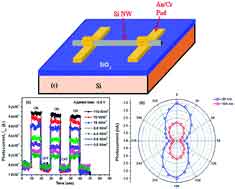 Silicon photosensors are semiconductor devices that convert light into electrical signals. They are widely used in digital cameras, optical communications, biomedical instruments, robotics, LiDAR systems, and industrial automation. Silicon-based photodetectors offer high sensitivity, low noise, and compatibility with CMOS fabrication processes.
Common Silicon Photosensor Technologies
- Photodiodes
- CMOS image sensors
- CCD image sensors
- Phototransistors
- Avalanche photodiodes (APDs)
- Silicon photomultipliers (SiPMs)
- Photovoltaic light sensors
- Graphene-enhanced photodetectors
Photodiodes
Photodiodes are among the most widely used silicon photosensors. They convert incident photons into electrical current through the photoelectric effect and are commonly found in optical communication systems, medical instruments, remote controls, and laser detectors.
Advantages of photodiodes include:
- Fast response times
- High sensitivity
- Wide spectral response
- Low noise operation
- Compatibility with integrated circuits
CMOS Image Sensors
CMOS image sensors dominate modern imaging applications because they provide high resolution, low power consumption, and fast signal processing. They are used in:
- Smartphone cameras
- Digital cameras
- Machine vision systems
- Medical imaging equipment
- Automotive cameras
- Industrial inspection systems
Graphene-Enhanced Silicon Photosensors
Graphene-based photodetectors are being investigated to improve sensitivity and extend wavelength detection beyond traditional silicon limits. Graphene-silicon hybrid devices show promise for:
- UV photodetectors
- Near-infrared sensors
- High-speed optical communications
- Flexible electronics
- Wearable sensors
Advantages of Silicon Photosensors
Silicon remains the most popular material for photosensors because it offers excellent performance and low manufacturing costs.
- High quantum efficiency
- Excellent response in the visible spectrum
- Low dark current
- CMOS compatibility
- Low production cost
- Long-term reliability
- High manufacturing yields
Limitations of Silicon Photosensors
Despite their advantages, silicon photosensors have several limitations:
- Reduced sensitivity in the infrared region
- Temperature dependence
- Limited UV response without specialized coatings
- Noise at very low light levels
- Saturation under extremely intense illumination
Photovoltaic Light Sensors
Photovoltaic light sensors generate electrical signals directly from incident light. These sensors are used for:
- Ambient light sensing
- Solar tracking systems
- Display brightness control
- Energy harvesting devices
- Industrial automation
Applications of Silicon Photosensors
- Digital cameras and image sensors
- Biomedical diagnostics
- Optical communication systems
- Laser detection
- Robotics and machine vision
- Autonomous vehicles
- LiDAR systems
- Consumer electronics
- Security systems
- Scientific instrumentation
Why Silicon is Ideal for Photosensors
High-quality silicon wafers provide excellent carrier mobility, low defect densities, and compatibility with semiconductor manufacturing processes. These characteristics make silicon the preferred material for fabricating photodiodes, CMOS image sensors, and advanced optical detectors.