
Si Wafers Used for Raman Micro-Spectrometry
Clients have used the following substrates for their Raman microspectrometry.
6" N/As (100) 675um SSP 0.001-0.005 ohm-cm
SEMI , 1Flat (57.5mm), Thermal Oxide 0.1μm±5% thick, Empak cst.
Get Your Raman Microspectrometry Substrate Quote FAST! Or, Buy Online and Start Researching Today!
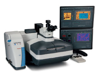
Raman Microscope
Below is a modern Raman microscope. This dispersive Raman system uses an Olumpus microscope and is equipped with interchangeable lasers and optics enabling operarations at 455, 532, 633 or 785nm.
Related Silicon Wafer Resources
What is Raman Spectrometry
Raman Micro-spectrometry is a form of scanning in which the sample is exposed to an electric field and the ultra-sonic vibration of atoms and molecules produces a reflection spectrum. The Raman spectrum is then used to create a map of the sample's vibrational structure which is termed as Raman function. In the modern applications, the method is utilized to measure the stress level of the sample through the Raman frequency measurement.

Silicon wafer research has moved from the realm of high tech electronic devices to a new area of study called "scalpel microscopy". The goal of this research is to examine micro-structures with a focus on the interface structures which connect these micro-structures. Microscopy is simply the science of viewing things at a very small level. We can use light, gas, electricity, and even chemical agents to view these tiny interfaces. The microscopes that enable us to do this are called light microscope and electron microscopes. There are many methods for using these microscopes.
When investigating the properties of silicon-based interfaces, we must understand the relationship between silicon and the various facets which compose the material. Silicon has a degree of electronic charge, which is called a p-n junction, which is a combination of N and S components. The silicon wafer used in many microscopy studies has a thickness that ranges between four to ten microns. This thickness will depend upon the characteristics of the coating being used on the surface.
Silicon Wafer Spectroscopy is typically conducted on unicellular materials. The silicon raman peak is the most valuable part of the silicon wafer, as this represents the crystalline structure of the material. The flake is a collection of negatively charged amino acids, which is encapsulated within a lattice which contains hydrogen atoms which have electron energy but no nucleus.
In microscopy studies of silicon substrate ramanite crystals, the normal view is that the crystal is made up of numerous prisms with the interior surface being smooth. But this coating doesn't just hide the interior topography - it actually makes the surface smoother than its real function might indicate. The reflection of light off the flat interior flake means that the reflectivity decreases as the number of facets increase. This is the reason why it is possible to use the absorption coefficient for determining the thickness of a semiconductor wafer. The higher the absorption coefficient, the thicker the silicon wafer.
As the number of facets increases, so does the thickness. The raman spectra shows the white color of a flat, smooth crystal. But as the number of facets increase, the white surface becomes more pronounced and can be seen to have an overall color that is blended into the background. This means that the thickness has a direct relationship to the white silicon peak intensity.
In order to determine the absorption coefficient, the light is shone on the crystal from above, below or at the same angle as the reflected light wave reaches it. Once this measurement is done, the results are displayed in units called mcg/cm. The value of the mcg/cm of the crystal can be compared with the standard value of u(h) by dividing the result by the number of inches. This value is important, as it indicates the level of loss of energy due to absorption. A lower value indicates a better quality of silicon.
Silicon carbide wafers are used in flat manufacturing, electronic circuits, telecommunications applications and thin-film transistor production. High-quality silicon wafers are also used for making high-quality optical fibers. The most common devices that make use of silicon carbide in their fabrication process are flat panels, solar cells, medical equipment, automobile windshields, automotive transmission shields and television displays. As indicated, flat panels and solar cells make up the majority of flat silicon wafer production; however, there are also numerous thin-film wafers that make up a small percentage of the entire production.
Thin-film wafers are made by passing a semiconductor electric current through the surface material of the wafer. An electrical charge then causes the material to become coated with crystalline silicon. The crystals allow the electricity to pass through the wafer, which then provides a smooth surface to the electrical wafer.