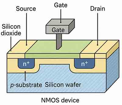
What Silicon Wafer Can Be Used to Make Negative-Channel Metal-Oxide Semiconductor NMOS devices?
We have the following silicon wafer item that is great for making NMOS devices.
Si Item #3193 - 100mm Undoped <100> >10,000 ohm-cm 525 micron Double Side Polished (DSP) with a Total Thickness Variation of 10 micron with TTV of 1um also available.

Low roughness for high-quality devices!
Please let us know if you can use or if you would like to us to quote you another spec.
Get your Quote Fast! Or, Buy Online and start researching today!
Silicon Wafers Fabricating Nmos Devices
Semiconductor devices are processes for the production of metal oxide semiconductors (MOS), which are used in everyday electrical and electronic devices as integrated circuit (IC) chips, which are present in all of them. In this process, they are manufactured just like an integrated circuit or IC chip, in which they form the core of the device. [Sources: 11]
The manufacturing process for SOI-MOS is the same as for silicon wafers, but it is much more complex. The manufacturing processes for SOI-MOS are similar to those of silicon wafers, except that they are embedded with a different material such as metal oxide semiconductors. [Sources: 1, 12]
Silicon wafers are produced through a series of repeated process steps, in which raw silicon is oxidized and various materials are deposited on the surface of the wafer. The first step is oxidation, which allows CMOS inverter fabrication (CMos) transistors to be produced on a printing press, after which different materials are deposited and etched into the photodiode sequence. This is then sent to a location where the raw silicone is transformed into a functioning chip. After the SOI wafer is turned upside down and glued to the silicone wafer, it is freed from its buried insulation layer to expose its semiconductor layer, and then the sequence is sequenced for CMOS manufacturing. [Sources: 1, 2, 4, 7]
The semiconductor component [300] may also contain a poly layer [318], which is formed by deposition on the surface of polycrystalline silicon. In other embodiments, semiconductors on a substrate [302] could contain or be added a layer of silicon oxide [323] or polysilica (PSAO) deposited and superimposed by a hemispherical Kuwaiti layer. [Sources: 3, 9]
If the SiGe substrate is present, it may also be advantageous to form a thin, stressed silicon layer (not shown) on the surface of the SiGe and oxidize the claimed silicon layer to form a silicon dioxide gate insulator. NMOS devices may also include localized halo regions that form a silicon-silicon alloy. This method, which is called silicon as an insulator technology, involves the use of silicon oxide and polysilicas in the form of a polylayer [323]. This is a layer of polycrystalline silicon on a high-thickness substrate [324] and an oxide layer on top [325]. [Sources: 0, 3, 11]
If the semiconductor substrate is a different semiconductor material from silicon, it may also be advantageous to deposit a gate insulator. A semicode electrical substrate can be a monocrystalline silicon material, but it is preferable to embed it with an asilicon-containing substrate, the term "asilicons substratea" here covering relatively pure silicon materials typically used in the silicon industry [325]. [Sources: 3]
Those who are familiar with this art will recognize that semiconductor substrates [36] can also be formed from a variety of other materials such as silicon germanium and silicon alloys [37]. In a host silicon material, a stress layer - inducing semiconductor material, for example, silicon - can be g germanium (SiGe), which has a surface area about 1,000 times that of silicon and consists of about 1.5 times that of any other material [38, 39]. Silicone and germ alloys - such as - a - semic chip alloys also have a high degree of thermal conductivity [40, 41, 42, 43]. [Sources: 0, 3]
The ability to generate stress - to induce materials in an epitaxially selective way - does not need to be described here, but will be known. Accordingly, CMOS transistor and gate design needs to be improved and the benefits of scaling achieved, while the poly-silicon depletion and exhaustion that occurs in conventional devices are avoided or reduced. The more circuits can be produced on silicon wafers, the smaller the transistors become, the cheaper the circuits become, and the lower the cost of making the transistor smaller and reducing the size of the circuit, which in turn leads to lower costs per circuit. [Sources: 3, 8, 10, 12]
First, the silicon wafers are bonded directly to a thermally grown and CVD-fabricated oxide layer on each wafer. Secondly, a thin layer of silicon dioxide grown on the wafers is heated to temperatures of up to 1,000 degrees Celsius. (3,500 degrees Fahrenheit) before it is bound to the oxide layers, which are thermally cultivated and produced by CVM. [Sources: 2, 5]
The thickness of BSI silicon wafers is less than 10 mm, and the IG forms an oxygen leak on the silicon crystal mass, which acts as a getter sink during the manufacturing process. The wafer also has a number of process-related defects, including metallic impurities and impurities resulting from thin rake and manufacturing processes. [Sources: 10]
It is well known that silicon MOS transistors can be subjected to compressive longitudinal voltage by embedding a material such as silicon germanium (SiGe) at the end of the transistor channel. The failure of scaled - downward corrected - CMOS devices with poly-silicon gate contacts is called poly-silicon depletion. [Sources: 3, 8]
In the Bell Labs experiment, the amorphous silicon did not pass the oxide step, so there is no reason why only discrete transistors could be produced, a process that is unsuitable for integrated circuits. When the monomer hydrogen is implanted in the silicon crystal mass, it remains in the mass for a long time. [Sources: 6, 10]
Sources
[0]: http://www.google.com/patents/US7391087
[1]: http://agrafik.is/m4lhk5/cmos-fabrication.html
[2]: https://www.techspot.com/article/1840-how-cpus-are-designed-and-built-part-3/
[3]: https://www.google.co.in/patents/US7326601
[4]: http://ptlbd.net/jeda/hybrid-ic-fabrication-process.html
[5]: http://www.appliedmaterials.com/nanochip/nanochip-fab-solutions/july-2014/thick-epitaxial-silicon-enhances-perfomance-of-power-and-mems-devices
[6]: http://www.intel4004.com/sgate.htm
[7]: https://patents.justia.com/patent/5497019
[8]: http://www.google.com.gi/patents/US7531400
[9]: https://www.google.com/patents/US9263445
[10]: https://www.ncbi.nlm.nih.gov/pmc/articles/PMC6540011/
[11]: https://newikis.com/en/Fabrication_(semiconductor)
[12]: https://www.design-reuse.com/articles/41330/cmos-soi-finfet-technology-review-paper.html
