Research Inquiry:
"Do you have m-plane (10-10) sapphire substrates available? If so, can I receive a formal quotation?"
Reference #270442 for specifications and pricing.
UniversityWafer supplies research-grade semiconductor wafers and substrates for device research laboratories, supporting projects in semiconductor device fabrication, MEMS, photonics, power electronics, RF devices, quantum technologies, and sensor development. Choose from silicon, sapphire, silicon carbide, gallium nitride, germanium, SOI, quartz, and specialty glass wafers in a wide range of sizes, orientations, and specifications for research and production.

UniversityWafer supplies research-grade semiconductor wafers and substrates for device research laboratories, universities, government research facilities, and commercial R&D organizations. Our customers use silicon, sapphire, silicon carbide, gallium nitride, germanium, quartz, and glass substrates for semiconductor device fabrication, MEMS, photonics, sensors, and advanced materials research.
One researcher requested the following m-plane sapphire substrate for a semiconductor device fabrication project:
Research Inquiry:
"Do you have m-plane (10-10) sapphire substrates available? If so, can I receive a formal quotation?"
Reference #270442 for specifications and pricing.
Get Your Quote FAST! Or, Buy Online and Start Researching Today!
Need a custom research substrate? Include your material, crystal orientation, wafer diameter, thickness, surface finish, and quantity in the form above, and our engineering team will recommend the best wafer for your research application.
A semiconductor device research laboratory is a facility dedicated to designing, fabricating, testing, and characterizing advanced electronic devices. Researchers work with materials such as silicon wafers, germanium, gallium nitride (GaN), silicon carbide (SiC), and sapphire substrates to develop next-generation semiconductor technologies.
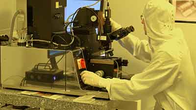 Device research laboratories combine material science, electrical engineering, and nanofabrication to improve the performance, efficiency, and reliability of electronic components used in computers, telecommunications, power electronics, sensors, medical devices, aerospace systems, and consumer electronics.
Modern semiconductor research laboratories investigate a wide variety of technologies, including:
Molecular doping is an advanced technique used to modify the electrical properties of semiconductor materials by introducing carefully selected dopant molecules. Researchers use molecular doping to improve carrier concentration, reduce contact resistance, optimize p-n junctions, and enhance charge transport in electronic and optoelectronic devices.
This process has become increasingly important for developing organic semiconductors, flexible electronics, high-performance transistors, and next-generation integrated circuits.
Semiconductor device laboratories rely on specialized equipment to fabricate and evaluate new materials and electronic devices. Common laboratory equipment includes:
The choice of substrate plays a critical role in semiconductor device performance. UniversityWafer supplies research-grade substrates for a broad range of device development projects, including:
UniversityWafer supplies semiconductor substrates to universities, government laboratories, startup companies, and commercial manufacturers worldwide. Whether your research focuses on power electronics, MEMS, quantum devices, photonics, sensors, RF components, or advanced integrated circuits, we can help identify the substrate that best fits your fabrication process.