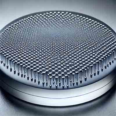
SoG for Optical Metasurface Fabrication
A physics and astronomy student requested a quote for the following:
I wish to buy a wafer of thin layers of silicon-on-glass, for optical metasurface fabrication. I wonder about several things:
- Where exactly in your website can I find this product?
- What is the possible thickness of the silicon layer? Can it be customized? I need about a 150 nm thick layer.
Reference #256054 for specs and pricing.
Get Your Silicon Wafer Quote FAST! Or, Buy Online and Start Researching Today!
Silicon-on-Insulator For Optical Metasurface Fabrication
A Physics PhD student requested a quote for the following:
Could we order a set of SOI wafers with the following specifications: Device Layer thickness: 1um Device layer resistivity: 10 Ohm.cm (or higher), Phosphorous-doped Box (oxide) thickness: 2um Handle Resistivity: 1000 Ohm.cm (or higher) We can take any wafer size - whatever will have the shortest lead time. Double side polished would be our preference, and we would be willing to pay more for this. However, if you only have single side polished, this also works. We would also be willing to pay more for shorter lead time. Looking forward to hearing back from you.
We are fabricating an optical metasurface, the resonators of which will be 910nm in height (hence the need for 1um device layer).
Could you send over the information about the 2um SOI you mentioned earlier? It may be possible for us to thin it down to 910nm.
Reference #275099 for specs and pricing.
What Is An Optical Metasurface?
An optical metasurface is a two-dimensional material engineered to manipulate light at subwavelength scales. These surfaces are composed of arrays of nanostructures, often called "meta-atoms," which interact with electromagnetic waves in a manner that traditional optical materials cannot achieve. Here are some key aspects of optical metasurfaces:
Key Characteristics:
- Subwavelength Features: The nanostructures are smaller than the wavelength of the light they
 manipulate.
- Tailored Optical Properties: By designing the shape, size, and arrangement of the meta-atoms, metasurfaces can achieve specific optical functions such as bending, focusing, or filtering light.
- Planar Configuration: Unlike bulk metamaterials, which are three-dimensional, metasurfaces are typically a single layer of nanostructures on a flat substrate.
Functionalities:
- Beam Steering: Metasurfaces can control the direction of light beams without the need for bulky lenses or mirrors.
- Lens Functionality: They can act as flat lenses, focusing light similarly to traditional curved lenses but in a much thinner form factor.
- Wavefront Shaping: The phase, amplitude, and polarization of light can be precisely controlled, enabling applications like holography and advanced imaging.
- Polarization Control: Metasurfaces can manipulate the polarization state of light, which is useful in optical communication and sensing.
Applications:
- Imaging Systems: Enhancing resolution and reducing the size of optical components.
- Communications: Improving the efficiency and functionality of optical communication systems.
- Sensing: Developing sensitive detectors for biological, chemical, and environmental sensing.
- Augmented and Virtual Reality: Creating compact and efficient optical components for headsets and other devices.
Design and Fabrication:
- Material Choice: Materials such as silicon, gold, silver, and titanium dioxide are commonly used for their favorable optical properties.
- Nanofabrication Techniques: Advanced lithography and etching techniques are used to create the precise nanostructures required for the desired optical effects.
Advantages:
- Compactness: Metasurfaces are much thinner and lighter than traditional optical elements.
- Versatility: A single metasurface can replace multiple optical components.
- Performance: Enhanced control over light propagation and interaction.
Challenges:
- Fabrication Precision: High precision is required in the fabrication process to achieve the desired optical properties.
- Scalability: Manufacturing large-area metasurfaces with uniform properties can be challenging.
- Losses: Minimizing absorption and scattering losses to ensure high efficiency.
Example:
A common example of an optical metasurface is a flat lens, or metalens, which can focus light without the curved surface of a traditional lens. By arranging nanostructures on a flat surface, the metalens can bend light rays to a focal point, achieving similar or even superior performance to conventional lenses but with a significantly reduced thickness.
Optical metasurfaces represent a significant advancement in photonics, offering new possibilities for miniaturizing and enhancing optical devices.

 manipulate.