
What Kind of Wafer is Used For Photonic Metamaterials Research?
Clients have used and confirmed that the following Silicon-on-Sapphire Wafer works best for Photonic Metal Materials research.
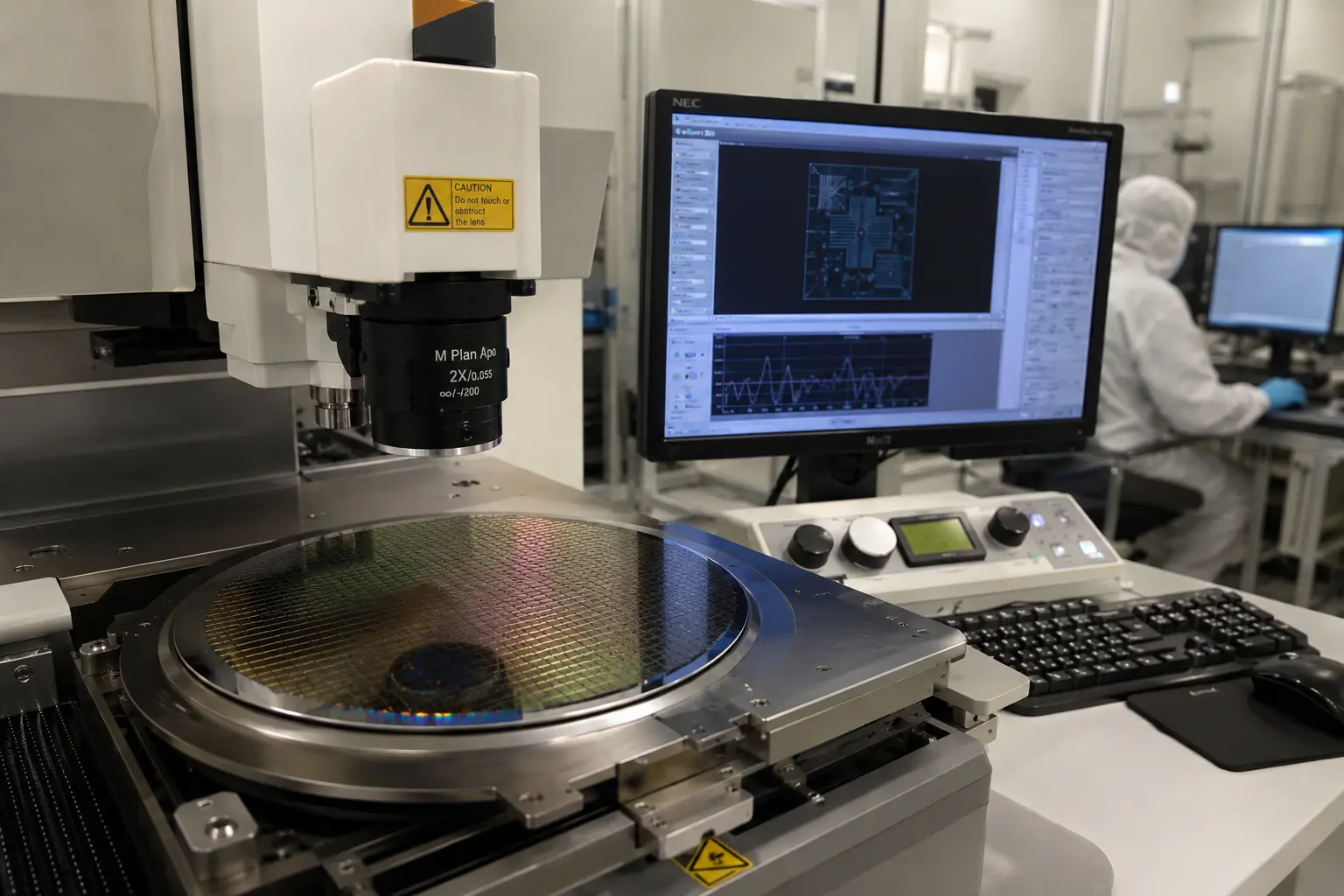
SOS, 4", R-plane+/-0.5° 460+/-20 DSP 0.6um <100
Please let us know if you can use or if you would like us to quote you on another spec?
In the last few years photonic metamaterials have experienced incredible gains in subwavelength-scale nanostructures with elaborately designed periodic and disordered photonic materials for applications in integrated photonics. Silicon-on-Sapphire is helping advance subwavelength engineering used in silicon photonic devices.
Researchers are using subwavelength gratings and hyperuniform disordered photonic structures to attain state-of-the-art performances for the near- and mid-infrared applications in:
- fiber-chip coupling
- slot waveguides for refractive-index sensing
- mode conversion
- wavelength filtering
- integrated resonators
- ultracompact high-extinction
- broadband integrated polarizers.
Get Your Silicon-on-Sapphire Wafer Quote FAST! Or, Buy Research Wafers Online Today .
Related Photonics Research Pages
Silicon-on-Sapphire for Photonic Metamaterials
Silicon-on-sapphire wafers are useful for photonic metamaterials research because they combine a silicon device layer with the optical, insulating, and thermal benefits of sapphire. This makes them helpful for integrated photonics, infrared optics, subwavelength structures, and advanced optical device development.
Photonic metamaterials are engineered materials designed to control how light moves through a structure. Instead of only relying on the natural properties of a material, researchers create small repeating or disordered features that interact with light at very small scales.
Can Electronic Chips Become Photonic Chips?
Electronic chips move information using electrons, while photonic chips move information using light. A photonic chip can guide photons through waveguides, resonators, filters, and other optical structures. This is why researchers are interested in combining electronics and photonics on the same chip.
To make these devices, engineers often start with high-quality silicon wafers or engineered substrates. Silicon is useful because it is already widely used in semiconductor manufacturing and can be patterned into very small optical structures.
Photonic chips may support faster data transfer, lower power use, compact optical sensing, and future quantum photonics research. They are also important for applications that need light control on a small chip-scale platform.
Photonic Metamaterials Research Applications
Photonic metamaterials are used in research areas where light must be controlled, filtered, guided, or confined. These structures can help researchers design compact optical devices for near-infrared, mid-infrared, sensing, and communication applications.
- Fiber-chip coupling
- Slot waveguides for refractive-index sensing
- Mode conversion
- Wavelength filtering
- Integrated resonators
- Broadband integrated polarizers
- Optical sensing devices
- Quantum photonics research
Subwavelength Structures and Integrated Photonics
Many photonic metamaterials use subwavelength structures, meaning the features are smaller than the wavelength of light they are designed to control. These structures can change how light bends, reflects, transmits, or becomes confined inside a device.
Researchers also use photonic devices to study waveguides, optical filters, resonators, and other chip-scale light-control structures. These applications often require low-defect substrates with consistent film quality and good surface finish.
Material Platforms for Photonic Metamaterials
Different wafer materials can be used depending on the optical wavelength, device design, and fabrication process. Sapphire wafers are valuable for optical and high-temperature applications, while SOI wafers are widely used for silicon photonics and optical waveguides.
Nitride on silicon wafers can also be useful for photonics applications such as sensing, LIDAR, frequency combs, telecommunications, and quantum photonics research.
Why Wafer Quality Matters
Photonic metamaterials often require precise patterning, smooth surfaces, and controlled film thickness. Small defects or surface irregularities can affect optical performance, especially when devices are designed for infrared, sensing, or resonator applications.
Choosing the right substrate helps researchers improve optical confinement, reduce losses, and support repeatable fabrication results. UniversityWafer, Inc. supplies research wafers for silicon photonics, metamaterials, MEMS, optical devices, and custom semiconductor projects.