
Wafers for Planar and Pattern Thin Film Research & Production
Planar and pattern film wafers offer a number of advantages over traditional manufacturing methods.
These film wafers allow for smaller, more densely packed circuit features. This leads to smaller devices with more functionality. Additionally, the technology is becoming the standard in the semiconductor industry, offering greater flexibility and a wider range of applications.
Get Your Planar & Pattern Film Wafer Quote FAST! Or, Buy Semiconductor Research Wafers Online Today .
Related Wafer Research Pages
- Silicon Wafers
- Spin Coating Silicon Wafers
- SOI Wafers
- Thermal Oxide Wafers
- Semiconductor Manufacturing
What Are Planar and Pattern Film Wafers?
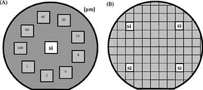
Planar and pattern film wafers are substrates used in semiconductor research, thin film deposition, lithography, and device fabrication. Planar film wafers usually have a smooth, uniform film surface, while pattern film wafers include defined structures or patterned features used to build smaller and more advanced devices.
Difference Between Planar and Pattern Film Wafers
Planar film wafers are often used when researchers need a uniform film layer for testing, coating, or deposition studies. Pattern film wafers are used when features, lines, or structures need to be added to the wafer surface for semiconductor, MEMS, photonics, or microelectronics applications.
Both wafer types are useful for manufacturing devices because they allow smaller and more densely packed circuit features. This can help create smaller devices with improved performance and more functionality on a single chip.
Thin Film Processing and Wafer Performance
Planar and pattern film wafers can be more complex to manufacture because thin film layers must stay uniform, stable, and properly aligned. As feature sizes become smaller, overlay accuracy, stress, distortion, and defect control become more important.
These wafers are commonly used with crystalline silicon, but they may also be produced on other substrates depending on the application. Non-silicon substrates can be useful for optical, high-temperature, RF, and advanced semiconductor research.
Photoresist Alignment and Lithography
The quality of a planar or pattern film wafer depends on how closely the photoresist image is aligned with the wafer surface. In pattern film lithography, the photoresist must be aligned with existing wafer features to create accurate device structures.
Laser writing and lithography methods can also be used to create patterns on the substrate. These processes help researchers control surface patterns, optical characteristics, and thin film structures.
Spin Coating for Thin Film Research
Spin coating is commonly used to apply uniform photoresist layers onto wafers. A consistent photoresist layer helps reduce defects and improves the quality of patterned thin film processing.
Spin coating is important when researchers need controlled film thickness, good surface coverage, and low defect density for semiconductor and microfabrication applications.
Applications for Planar and Pattern Film Wafers
- MEMS device fabrication
- Photolithography research
- Semiconductor process development
- Thin film deposition studies
- Microelectronics packaging
- Optoelectronic device research
Typical Wafer Specifications
| Parameter | Options |
|---|---|
| Wafer Diameter | 50mm, 100mm, 150mm, 200mm |
| Substrate Types | Silicon, Sapphire, Quartz, SiC |
| Film Types | Oxide, Nitride, Metal, Photoresist |
| Orientation | <100>, <111> |
| Surface Finish | SSP, DSP |