Silicon Fabrication Methods | UniversityWafer, Inc.
Silicon fabrication methods are the foundation of modern semiconductor manufacturing, enabling the production of silicon wafers, integrated circuits, MEMS devices, sensors, photonic components, and solar cells. Processes such as crystal growth, photolithography, thermal oxidation, wafer polishing, doping, and layer transfer allow engineers to transform raw silicon into high-performance electronic devices. Understanding these fabrication techniques is essential for researchers and manufacturers developing next-generation semiconductor technologies.
Silicon Fabrication Laboratory Materials
Modern silicon fabrication laboratories require high-quality substrates for photolithography, wafer bonding, MEMS fabrication, microfluidics, semiconductor packaging, and device prototyping. In addition to silicon wafers, researchers frequently use quartz, fused silica, sapphire, and specialty glass substrates for process development and advanced semiconductor research.
A process engineer requested a quote for the following wafer specifications:
I'm looking for some quartz wafers with the following specifications:
The wafers must include a SEMI flat because they will be processed using a mask aligner that requires flat-edge wafer loading.
Reference #140016 for specifications, availability, lead times, and pricing.
Why Silicon Is Used in Semiconductor Fabrication
Silicon is the second most abundant element in the Earth's crust and remains the foundation of modern semiconductor technology. Its unique electrical properties, ability to form high-quality silicon dioxide, and compatibility with advanced manufacturing processes make it the preferred material for integrated circuits, sensors, MEMS devices, power electronics, and solar cells.
Virtually every smartphone, computer, automotive control system, medical device, and communication network relies on semiconductor components fabricated on silicon wafers. As a result, silicon wafer fabrication continues to be one of the most important manufacturing technologies in the world.
Common Silicon Fabrication Methods
The production of semiconductor devices involves multiple fabrication processes, including:
Crystal Growth and Ingot Production
Wafer Slicing and Polishing
Photolithography
Thermal Oxidation
Doping and Ion Implantation
Thin Film Deposition
Etching and Pattern Transfer
Wafer Bonding and Layer Transfer
Packaging and Testing
Each step contributes to the performance, reliability, and yield of the final semiconductor device. Advanced fabrication methods allow manufacturers to create billions of transistors on a single silicon wafer while maintaining exceptional precision and consistency.
UniversityWafer supplies research-grade silicon wafers, quartz substrates, glass wafers, SOI wafers, thermal oxide wafers, and custom semiconductor materials for universities, laboratories, and commercial fabrication facilities worldwide.
Silicon Fabrication Methods
Silicon fabrication methods are the processes used to transform raw silicon into polished wafers, semiconductor devices, integrated circuits, MEMS structures, and solar cells. These methods include crystal growth, wafer slicing, grinding, polishing, photolithography, oxidation, deposition, etching, doping, and layer transfer. Each step must be carefully controlled to produce wafers with the correct orientation, thickness, surface finish, flatness, and electrical properties.
Silicon remains the most widely used semiconductor material because it can form high-quality silicon dioxide, supports advanced lithography, and is compatible with high-volume wafer processing. Researchers and manufacturers use these fabrication techniques to create microchips, sensors, power devices, photonic devices, and laboratory research substrates.
Photolithography is one of the most important steps in semiconductor fabrication. It uses light, photoresist, and patterned masks to transfer circuit designs onto a silicon wafer. The wafer is coated with photoresist, exposed to ultraviolet light through a photomask, developed, and then etched or implanted to create precise device patterns.
This process allows manufacturers to build transistors, integrated circuits, MEMS devices, microfluidic features, and nanoscale structures on a single wafer. As device dimensions continue to shrink, photolithography remains essential for producing high-density chips and advanced semiconductor devices.
Thermal Oxidation of Silicon Wafers
Thermal oxidation grows a controlled layer of silicon dioxide (SiO2) directly on the silicon wafer surface. This oxide layer can act as an electrical insulator, surface passivation layer, diffusion barrier, etch mask, or dielectric material for semiconductor devices.
During oxidation, silicon reacts with oxygen or water vapor at high temperature to form SiO2. Dry oxidation is often used for thin, high-quality oxide layers, while wet oxidation is commonly used when faster oxide growth or thicker films are required. Thermal oxide wafers are widely used in MEMS, MOS devices, photolithography, sensors, and research applications.
Grinding, Lapping, and Polishing Silicon Wafers
Silicon wafer fabrication requires precise mechanical processing to achieve the correct thickness, flatness, and surface roughness. Grinding and lapping remove material from the wafer, while polishing improves surface quality for device fabrication. Silicon carbide abrasives are commonly used because of their hardness and durability.
After slicing an ingot into wafers, manufacturers use edge grinding, surface grinding, chemical mechanical polishing (CMP), and cleaning steps to prepare the wafer for semiconductor processing. These steps help reduce surface damage, control total thickness variation, and produce prime-grade, test-grade, or mechanical-grade wafers.
Layer Transfer and SOI Wafer Fabrication
Layer transfer techniques are used to move a thin silicon layer from one wafer to another. These methods are important for producing silicon-on-insulator (SOI) wafers, thin silicon membranes, bonded wafers, and specialty substrates.
In SOI wafer fabrication, a thin device layer of silicon is separated from the bulk substrate by an insulating oxide layer. This structure improves electrical isolation, reduces parasitic capacitance, and supports high-performance electronics, MEMS, RF devices, and photonic applications.
Silicon Crystal Growth Methods
Before wafers can be processed, high-purity silicon must be grown into single-crystal ingots. Crystal growth methods determine wafer quality, crystal orientation, oxygen content, defect density, and electrical performance. The most important silicon crystal growth methods include the Czochralski method, float-zone growth, Bridgman growth, and gradient freeze techniques.
Czochralski Silicon Growth
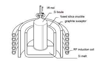
The Czochralski method is one of the most common techniques for producing single-crystal silicon ingots. A seed crystal is dipped into molten silicon and slowly pulled upward while rotating. This forms a cylindrical silicon ingot with controlled crystal orientation and dopant concentration.
After growth, the ingot is cropped, ground, sliced into wafers, etched, polished, inspected, and packaged. Czochralski-grown silicon is widely used for integrated circuits, power devices, MEMS, sensors, and solar applications.
Bridgman and Gradient Freeze Methods
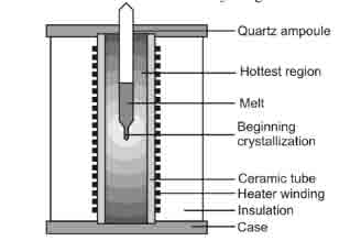
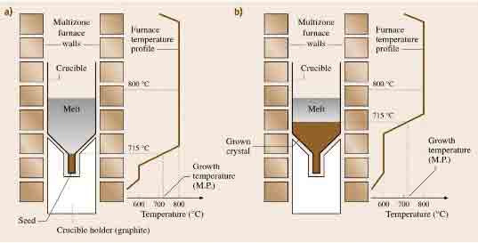
The Bridgman method and gradient freeze method are directional solidification techniques used to grow crystals by carefully controlling the temperature gradient between molten and solid material. These methods are important in crystal growth research and are also used for several compound semiconductor materials.
Careful control of temperature, seed orientation, cooling rate, and impurity concentration helps reduce crystal defects and improve wafer performance. These crystal growth techniques support research in semiconductor materials, optoelectronics, sensors, and advanced wafer development.
Why Silicon Fabrication Methods Matter
Every silicon wafer fabrication step affects the final wafer's performance. Crystal growth controls material purity and orientation, slicing defines wafer geometry, polishing improves surface quality, photolithography creates device patterns, oxidation forms dielectric layers, and layer transfer enables advanced wafer structures. Choosing the correct fabrication method is essential for semiconductor manufacturing, microelectronics, MEMS, photonics, solar cells, and materials research.
Crystal Growth References
Avadhanulu M.N. & Murthy, A. T. A Textbook of Engineering Physics. S. Chand Publishing.
Govindhan Dhanaraj, K. B. Springer Handbook of Crystal Growth. Springer Science & Business Media.
Kuphaldt, T. R. Lessons In Electric Circuits, Volume III – Semiconductors.