Fabricating Microchips with a Polysilicon Gate Structure
A physics student contacted UniversityWafer for help selecting a suitable
silicon wafer with a polysilicon gate layer for an early-stage
microchip fabrication project.
Researcher's Request
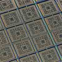 We would like to fabricate microchips using a
polysilicon gate structure.
Based on our current process, we believe we need a
p-type silicon wafer
with a <100> crystal orientation.
Because the project is still in its early stages, we may be able to adjust the process if another substrate configuration is more practical.
We would like to fabricate microchips using a
polysilicon gate structure.
Based on our current process, we believe we need a
p-type silicon wafer
with a <100> crystal orientation.
Because the project is still in its early stages, we may be able to adjust the process if another substrate configuration is more practical.
We are specifically looking for a p-type, <100>-oriented silicon wafer with
polysilicon deposited on the surface. Could you provide information about the
substrate orientation, dopant type, resistivity, and deposited polysilicon specifications?
UniversityWafer Can Help Specify the Correct Wafer
UniversityWafer can supply custom silicon and polysilicon wafer structures
for transistor, MOS capacitor, integrated-circuit, MEMS, and university research.
Important specifications should be selected according to the planned oxidation,
photolithography, implantation, diffusion, etching, and metallization processes.
For a polysilicon-gate project, the quotation request should include:
- Wafer diameter
- P-type or n-type conductivity
- Dopant species
- Crystal orientation, such as <100> or <111>
- Substrate resistivity
- Wafer thickness
- Single-side or double-side polishing
- Thermal oxide thickness, when required
- Polysilicon film thickness
- Undoped or doped polysilicon
- Requested wafer quantity
Reference #274460 for specifications and pricing.
Why Are Microchips Made from Silicon?
Most microchips are fabricated on
silicon wafers
because silicon combines controllable electrical conductivity, thermal stability,
mechanical strength, a high-quality native oxide, and compatibility with mature
semiconductor manufacturing processes.
Silicon is neither a good conductor like copper nor a strong insulator like glass.
Instead, it is a semiconductor whose electrical properties can be
carefully modified through doping. This makes it possible to create the p-type and
n-type regions used in diodes, transistors, integrated circuits, image sensors, and
many other electronic devices.
Request Your Silicon Wafer Quote FAST!
Tell us your wafer diameter, crystal orientation, conductivity type, resistivity,
polishing requirement, oxide thickness, polysilicon thickness, and quantity. We can
help identify an appropriate substrate for your semiconductor fabrication process.
Or,
Buy Online
and Start Researching Today!
Important Silicon Wafer Specifications for Microchips
Device performance and fabrication yield depend on more than the wafer's conductivity
type. Surface flatness, crystal quality, cleanliness, resistivity, orientation, and
polishing quality all affect photolithography, thin-film deposition, etching, bonding,
and device uniformity.
| Wafer Specification |
Why It Matters |
| Total Thickness Variation (TTV) |
Measures the difference between the thickest and thinnest points across the wafer.
Low TTV helps maintain focus and uniform processing during photolithography.
|
| Bow |
Describes the curvature of the wafer relative to its center plane. Excessive bow
can interfere with handling, coating, exposure, and bonding.
|
| Warp |
Measures overall wafer distortion. Low warp is important for process-tool
compatibility and accurate pattern transfer.
|
| Surface roughness |
A smooth polished surface supports uniform oxide growth, thin-film deposition,
lithography, and interface quality.
|
| Crystal orientation |
Orientations such as <100> and <111> influence oxidation, carrier
behavior, etching, and device processing.
|
| Resistivity |
Resistivity reflects dopant concentration and helps determine the wafer's
electrical behavior in the finished device.
|
| Polishing |
Prime-grade device fabrication generally requires a highly polished,
low-defect surface.
|
UniversityWafer supplies silicon wafers with low TTV, bow, and warp specifications,
including selected wafers with approximately 1 μm, 2 μm, or 5 μm TTV,
depending on diameter, grade, and availability.
How Silicon Transistors Work as Electronic Switches
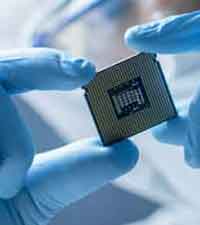 Engineers use silicon to fabricate microscopic gates, channels, junctions, and switches.
A transistor controls the movement of electrical charge and can represent an on or off
state in a digital circuit. Modern processors and memory devices contain extremely large
numbers of transistors integrated onto a single chip.
Engineers use silicon to fabricate microscopic gates, channels, junctions, and switches.
A transistor controls the movement of electrical charge and can represent an on or off
state in a digital circuit. Modern processors and memory devices contain extremely large
numbers of transistors integrated onto a single chip.
These transistor switches perform the logical and mathematical operations used by CPUs,
memory chips, microcontrollers, communication devices, and other electronic systems.
High-quality
semiconductor wafers
provide the foundation on which these device structures are fabricated.
What Is a Polysilicon Gate?
A polysilicon gate is a patterned layer of polycrystalline silicon used
to control the conductive channel in a MOS transistor. The polysilicon may be deposited
by chemical vapor deposition and then doped to reduce its electrical resistance.
Although many advanced semiconductor processes now use metal-gate and high-k dielectric
structures, polysilicon gates remain important in education, legacy CMOS processing,
sensors, MEMS, test structures, and semiconductor research.
Is Silicon a Semiconductor?
Yes. Silicon is a semiconductor because its electrical conductivity falls between that
of a conductor and an insulator. Its conductivity can be adjusted by introducing small,
controlled amounts of dopant atoms.
Boron is commonly used to produce
p-type silicon,
while phosphorus, arsenic, or antimony may be used to produce
n-type silicon.
Combining p-type and n-type regions enables the fabrication of diodes, transistors,
integrated circuits, photovoltaic cells, and image sensors.
Silicon Wafers for CCD and Image Sensor Fabrication
Silicon is widely used in charge-coupled devices (CCDs), CMOS image sensors, photodiodes,
and visible-light detectors because photons can generate mobile charge carriers within
the semiconductor. Device designers select wafer resistivity, thickness, orientation,
doping, and surface quality according to the desired sensitivity and operating wavelength.
Why Is Silicon Widely Used in Semiconductor Electronics?
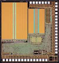 Silicon is the dominant material used to manufacture semiconductor chips, integrated circuits, transistors, sensors, and photovoltaic devices. Its success is not based on one property alone. Silicon combines controllable electrical conductivity, thermal stability, a useful band gap, strong mechanical properties, abundant raw materials, and a highly developed manufacturing infrastructure.
Pure silicon has limited conductivity, but its electrical behavior can be precisely modified through doping. Adding controlled amounts of donor or acceptor atoms creates n-type silicon or p-type silicon. This allows engineers to build the junctions, channels, gates, and switching structures required for modern semiconductor devices.
Key Reasons Silicon Is Used for Semiconductor Chips
| Silicon Advantage |
Why It Matters in Semiconductor Manufacturing |
| Controllable conductivity |
Silicon can be doped with elements such as boron, phosphorus, arsenic, or antimony to produce precise electrical properties. |
| Useful band gap |
Silicon has a room-temperature band gap of approximately 1.12 eV, which provides a practical balance between electrical control and operating temperature. |
| High-quality native oxide |
Silicon forms stable silicon dioxide, which is valuable for electrical insulation, surface passivation, MOS structures, and device isolation. |
| Thermal stability |
Silicon wafers tolerate many high-temperature oxidation, diffusion, annealing, and deposition processes used during chip fabrication. |
| Mechanical strength |
Single-crystal silicon can be processed into thin, flat wafers while maintaining the structural integrity needed for automated manufacturing. |
| Abundant raw material |
Silicon is abundant in the Earth's crust, primarily in silica-containing minerals such as quartz. |
| Mature fabrication technology |
Decades of investment have created highly optimized equipment and processes for growing, polishing, patterning, doping, and testing silicon wafers. |
| Scalable wafer production |
Silicon is available in standardized diameters and grades for research, pilot production, and high-volume semiconductor manufacturing. |
Silicon's Electrical Properties
Silicon is a semiconductor, meaning its conductivity lies between that of a conductor and an insulator. Its conductivity can be changed using doping, light, heat, or electric fields. This controllability makes silicon ideal for electronic switches such as MOSFETs, which form the foundation of processors, memory devices, power-management circuits, and digital logic.
In an undoped or intrinsic silicon wafer, electron and hole concentrations are relatively low. Doping introduces additional charge carriers and shifts the Fermi level, enabling engineers to tailor resistivity and carrier concentration for a specific device design.
The Importance of Silicon Dioxide
One of silicon's greatest manufacturing advantages is its ability to form a stable layer of silicon dioxide (SiO2). This oxide can be grown thermally or deposited as a thin film and is widely used for:
- Gate insulation in MOS devices
- Surface passivation
- Electrical isolation
- Diffusion masking
- Protective coatings
- MEMS and microfabrication processes
Although advanced transistors often use high-k gate dielectrics, silicon dioxide remains important in semiconductor processing because it forms a well-controlled interface with silicon.
Why Silicon Wafers Are Economical
Silicon does not normally occur in nature as pure elemental silicon. It is commonly found in compounds such as silica and silicates and must be refined to semiconductor-grade purity. Despite the purification required, silicon remains economical because the raw material is abundant and its manufacturing processes are highly standardized.
Large single-crystal ingots can be grown using methods such as the Czochralski process or float-zone crystal growth. These ingots are sliced, lapped, etched, polished, cleaned, and inspected to produce highly uniform silicon wafers.
Silicon Wafer Quality for Microchip Fabrication
Microchip yield depends heavily on wafer surface quality and dimensional uniformity. Important specifications include:
- Total Thickness Variation (TTV)
- Bow
- Warp
- Surface roughness
- Crystal orientation
- Resistivity
- Particle and defect density
- Edge profile
Low TTV, bow, and warp help keep the wafer properly aligned during photolithography, deposition, etching, bonding, and metrology. Prime-grade silicon wafers are commonly selected for device fabrication because they provide tighter flatness, cleanliness, and surface-finish specifications than lower-cost test-grade material.
Common Silicon Wafer Orientations
| Orientation |
Common Uses |
| <100> |
CMOS devices, MOS capacitors, integrated circuits, MEMS, and processes requiring high-quality oxide interfaces. |
| <111> |
Wet anisotropic etching, MEMS structures, epitaxial studies, and specialized device fabrication. |
| <110> |
Research involving carrier mobility, vertical structures, specialized MEMS, and advanced transistor designs. |
For many microchip projects, a <100> silicon wafer is preferred because of its compatibility with MOS processing and thermal oxide formation.
Applications of Silicon Semiconductor Wafers
- Microprocessors and central processing units
- Memory chips
- CMOS image sensors
- Power-management integrated circuits
- MEMS devices
- Photodiodes and photodetectors
- Solar cells
- Radio-frequency integrated circuits
- Analog and mixed-signal devices
- Microcontrollers
- Automotive electronics
- Medical and industrial sensors
Why Not Use Another Semiconductor Material?
Silicon is not the best material for every application. Compound and wide-bandgap semiconductors can outperform silicon under specific conditions. However, they are generally more expensive, more difficult to manufacture, or supported by a smaller fabrication ecosystem.
| Material |
Advantages |
Why It Has Not Replaced Silicon Broadly |
| Silicon |
Low cost, mature processing, excellent oxide, scalable wafer sizes, broad device compatibility. |
Performance is limited in some high-power, high-frequency, and high-temperature applications. |
| Silicon Carbide |
Wide band gap, high breakdown field, high thermal conductivity, excellent power-device performance. |
Higher wafer cost, harder material, more difficult crystal growth, and more demanding processing. |
| Gallium Arsenide |
High electron mobility and strong optoelectronic performance. |
Higher cost, brittle wafers, smaller manufacturing ecosystem, and limited native oxide quality. |
| Gallium Nitride |
Excellent for high-frequency, high-power, RF, and optoelectronic devices. |
More complex epitaxy, substrate mismatch challenges, and higher manufacturing cost. |
| Germanium |
High carrier mobility and infrared sensitivity. |
Smaller band gap, greater leakage current, and weaker oxide properties. |
Silicon and Next-Generation Semiconductor Technology
Silicon will continue to dominate mainstream semiconductor manufacturing because of its cost, availability, reliability, and mature infrastructure. At the same time, manufacturers increasingly combine silicon with other materials to improve performance.
Examples include silicon-on-insulator (SOI), epitaxial silicon, strained silicon, germanium-on-silicon, silicon photonics, and compound semiconductor layers integrated onto silicon substrates.
Rather than completely replacing silicon, many next-generation technologies use it as a mechanically stable, affordable, and fabrication-compatible platform.
Related Silicon Semiconductor Resources
