Fabricating Dielectric Mirrors
A physics professor requested a quote for the following:
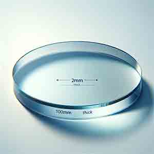
We are looking for Germanium substrates with 1"
diameter and a thickness of 0,25“=0.63mm.
Can you provide us a quote of the following?
- Plane/plane substrates
- Plane/concave ROC=-2000mm
We need a polished surface. We want to put dielectric mirror coating on it. It will be used as a mirror for lasers.
UniversityWafer, Inc. Quoted:
We think what you need is 0.25"(6.35mm) thick, not 0.63mm thick, we can not do Germanium Lens, please see our quotation for as cut blank below:
Ge Blank
Monocrystalline, N type, 5-40 ohm-cm
Size: Diam 1"x0.25"
Surface as cut
Reference #169527 for specs and pricing
Get Your Quote FAST! Or, Buy Online and Start Researching Today!
Fabricating Dielectric Mirrors
A PhD in Quantum Optics requested a quote for the following:
I am interested in double side polished Si wafer (possibly undoped). Ori 100 is OK. I need very  small roughness substrate ( < < 1 nm rms if it is possible).
I’ll try in explaining better my requirements.
I need to fabricate single photon sensors from thin films (5-8 nm) of NbN, NbTiN. For increasing the absorptance in such thin films I need to realize an optical cavity stack underneath by using multilayer DBR (dielectric mirror) and a quarter wavelength optical cavity with a layer of SiO2 (about 270 nm for working at 1550 nm). I mean a structure like that shown in the attached picture.
We could discuss about the number of multilayers (no more than 2-3) and material (Ta2O5 ?). Are you able to provide absorptance simulation? Of course the final roughness should be << 1nm.
 Anyway, I would like that the high absorptance will be maintained down to 1200 nm (because there are some interesting experiments where we need to work at that wavelength). Also I would like that below the 1000 nm wavelength the reflectivity of the DBR will be as low as possible because I need to use a laser passing trough it for aligning some stuff on the chip. For this reason I would like to use a Si wafer having thickness as small as possible (400 um) and double side polished. Anyway I would like that the final chip will be diced by you in sample of 10x10 square mm.
On the chip you will provide us we will deposit by DC reactive magnetron sputtering technique the 5-6 nm NbN or NbTiN film (800 C hating?) and we will also use EBL technique for patterning the device. This means that the whole chip will will be “heated” up to 180 C (but I don’t think this would be a problem) and also we will use reactive (CF4 gas) ion etching (RIE) for the patterning of the device. These are the factors at which the coating should survive. I think this should not be a problem because routinely people make this.
Please reference #213818 for specs and pricing.
Lithium Niobate Substrates to Fabricate Dielectric Mirror
A mechanical engineer requeted a quote for the following:
Do you do dielectric mirror coatings for lithium niobate? I would like to provide a 1” 0.3 mm thick X-cut LN wafer and have the following done: 1. Dielectric stack coating on each side for 1550 nm a. Side 1 reflection coeff.: 0.996 b. Side 2 reflection coeff.: 0.994 2. Diced for 3x3 mm samples.
Reference #268191 for specs and pricing.
What Substrates are Often Used to Fabricate Dielectric Mirrors?
Dielectric mirrors, also known as Bragg mirrors, are fabricated using multiple layers of dielectric materials on a substrate. The choice of substrate and dielectric materials can vary depending on the intended application and required properties of the mirror. Common substrates used for fabricating dielectric mirrors include:
-
Glass: Glass substrates are widely used due to their transparency, thermal stability, and ease of handling. They are suitable for a wide range of wavelengths and are commonly used in optical applications.
-
Silicon: Silicon substrates are often used for infrared applications. They offer good thermal conductivity and are compatible with standard semiconductor fabrication processes.
-
Fused Silica: Fused silica substrates are preferred for applications requiring high UV transmittance and low thermal expansion. They are highly pure and have excellent optical properties.
-
Sapphire: Sapphire substrates are used in applications requiring high thermal and mechanical durability. They are suitable for high-power laser applications due to their high melting point and thermal conductivity.
-
Quartz: Quartz substrates are chosen for their low thermal expansion and good UV transmission. They are often used in precision optical applications.
-
Plastic or Polymer: For more flexible applications, plastic or polymer substrates can be used. They are lightweight and can be easily shaped but are generally less durable and have lower thermal stability.
The choice of substrate is crucial as it must support the deposition of multiple thin dielectric layers while maintaining the overall structural integrity and performance of the mirror. The substrate material is selected based on factors like operating wavelength range, thermal properties, mechanical strength, and the intended application environment.
