How to Measure Silicon Wafer Resistivity with Four Point Probe

university wafer substrates

Four Point Probe

A postdoc requested an answer to the following question:

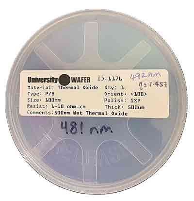
I am looking to purchase a wafer that can be used as a 4 point colinear measurement standard. Meaning that we have a known material of a certain size with a known sheet resistance.

UniversityWafer Replied:

I suggest to use the wafers with the narrowest resistivity ranges. We offer them in practically each resistivity range.

Reference #245648 for specs/pricing.

Get Your Quote FAST! Or, Buy Online and Start Researching Today!


CAPTCHA Image


Silicon Wafer Resistivity

We have a large selection of guaranteed resistivity range from low to highly doped, CZ and Float Zone.

Get Your Quote FAST! Buy Online and Start Researching Today!

Silicon Wafer Used for Four Point Probing

PhDs and other researchers use the four-point probing method to measure the resistance that varies with electrode location relative to sample boundary. Four-point probes are also used to measure sheet resistances of semiconductor thin films. The 4-point probe technique is a relatively straightforward, reliable technique which allows the measurement of thin films.

A director of engineering at a startup requested a substrate to test a four point probe.

I am looking for standard film thickness test wafers with Copper and one with Chromium..  Specifically for Cr and Cu.  4” or 6” are okay.  This is so that we can check our metal film thickness tool – a 4-point probe. One wafer of each as a calibration check for electrical 4-point probe. 

Doesn’t matter which type of wafer as it will have an oxide insulating layer before the top metal layer. As mentioned below, only one of each. 

We want to use them to measure our 4-point probe. We had bought an oxide test wafer from you (see image below) with a known oxide thickness.  Likewise, I am looking for reference wafers with known thicknesses of Cu and Cr.

researcher uses substrate to test four point probe

I need ~0.5um of Cu on oxide and 0.5um of Cr on oxide.  Wafer size doesn’t matter though I’d prefer a 3” or 4”.

UniveristyWafer, Quoted:

In-situ sputter etch followed by sputter  
deposition of 10nm Cr and 500nm Cu onto
one side of customer wafers.
Lot = 12 wafers, 100mm dia., or 15 wafers,
3" dia.
Qty 1 lot $
Price does not include the wafers

In-situ sputter etch followed by sputter Note 1 Note 2 1 lot 510.00 510.00
deposition of 500nm Cr onto
one side of customer wafers.
Lot = 12 wafers, 100mm dia., or 15 wafers,
3" dia.

Qty 1 lot $

Reference #266809 for specs and pricing.

Watch Video

Below are just some of the key terms associated with four point probe.

  • probe resistance
  • resistance measurements
  • probe technique
  • probe method
  • voltage probes
  • electric resistivity
  • contact resistances
  • measured resistance
  • conductivity test  
  • conductive coatings
  • wafer resistivity
  • sample thickness 
  • anisotropic systems
  • test methods
  • material resistivity    

Is A Silicon Wafer's 4 Point Probe Method Resistivity Value Measured from the Polished Surface?

A researcher associate studying mechanical and industrial engineering asked the following question:

Question:

I'd like to use Silicon wafer as a standard for checking the accuracy of a 4 point probe resistivity measurement station. We have Si wafers (10 - 20 ohm-cm) available formerly purchased from UniversityWafer.com. The resisivity values I measured are within the range of reported values for that set of wafers. However, the experiment sample I'd like to measure has resistivity value in the order of 0.01 ohm-cm. That's why I send inquires and would like to purchase wafers in the range of 0.01-0.02 ohm-cm.

Answer:

A silicon wafer ideally has the same resistivity throught its body. It certainly has the same resistivity on both sides, at the surfaces and within it. Radially there is some variation but for (100) orientation and (0.01-0.02) resistivity range, Radial Resistivity Variation is typically <5%.

By Chemical Vapor Deposition, one grows Silicon Epi layers on Silicon wafers, specifically for the purpose of creating silicon layer with different resistivities or different dopants, hence type, even to create p-n or n-p junctions.

One uses a 4 point probe to measure resistivity on Silicon ingots and on Silicon wafers before they are polished. A 4 point probe would mar the polished surface so for that one uses a no-contact resistivity gauge which induces current within the wafer and measures resultant energy dissipation, without touching the surface. Such gauges are good only for narrow ranges of resistivity and need to be calibrated with wafers of known resistivity, as measured by a 4 point probe.

Reference #201601 for specs and pricing.

How is Four Point Probing Used on Silicon Substrates?

Four-point probing is a technique used to measure the electrical resistivity of thin films and silicon substrates. It involves applying a potential difference across four contacts made to the sample and measuring the resulting current flow.

Here's how four-point probing is typically performed on silicon substrates:

  1. Preparation: A clean and flat silicon substrate is prepared and metallized at four equidistant points to form the four probe contacts.

  2. Probe Placement: The probe tips are positioned at the four metallized points on the substrate and a small current is passed through two of the probes to verify that the contacts are properly made.

  3. Resistance Measurement: A potential difference is applied between the two inner probes and the resulting current flow is measured using a high-impedance current amplifier. The resistance of the silicon substrate can then be calculated using Ohm's law (R = V/I).

  4. Repeatability: The resistance measurement is repeated several times to confirm the accuracy and reproducibility of the results.

  5. Analysis: The electrical resistivity of the silicon substrate can be determined from the measured resistance, taking into account the geometric dimensions of the sample and the distance between the probe contacts.

Four-point probing is widely used in the semiconductor industry for quality control and process monitoring. It is a non-destructive technique that provides precise and accurate measurements of the electrical resistivity of silicon substrates and thin films.

How to Determine a Silicon Wafer's Resistivity?

If you are trying to determine how to measure silicon wafer resistivity, you should know that the method involves using a temperature coefficient as the reference. To find the value of this parameter, you need to measure the resistance of a sample at a known temperature. Then, multiply the result by the film thickness. Repeat the measurements for the remaining samples. Before you begin, remember to disconnect the power strip and the table.

Methods Used to Measure Silicon Resistivity

measuring silicon wafer resistivityOne of the methods to measure the resistivity of silicon wafers is to use an MDPingot or MDPmap. These tools have a high resolution of 1 mm and can also measure minority carrier lifetime and surface flatness. The device can be used to measure the thickness of a silicon wafer, as long as it is more than 16 mm in diameter. Before you can determine the resistivity of silicon, you need to know the thickness of the silicon wafer.

Once you know the thickness of your silicon wafer, you can measure its resistivity. You must give the resistivity of the base material. You can also map the sheet resistance of a material. This method is often used to investigate the homogeneity of emitter diffusion. Using the four-point probe method, you can determine how much resistance is in a material. You must supply the thickness of the silicon wafer in order to measure the resistivity.

What is a Tensile Resistivity Tester

If you want to measure the resistivity of silicon wafers, you should learn the simplest method and start by reading the data in a tensile resistivity tester. Then, you need to measure the resistance of a wafer to see if it matches the resistance of your material. This measurement method is called the "four-point probe technique". To find the resistivity of a silicon wafer, you must take its thickness into account.

There are many methods of measuring the resistance of silicon wafers. The most common is the four-point probe method. There are several advantages to this method. It allows you to measure the resistivity of a material at various levels. However, this method is only suitable for thin films. It can't measure the thickness of a silicon wafer. This technique requires the use of a multi-point electrode.

To measure the resistivity of a silicon wafer, you need to first identify the thickness of the wafer. Then, you need to determine the thickness of the silicon. You should take the thickness of the silicon and the resistance of the metal. Depending on the thickness, you will need to measure the resistivity of the silicon. You will need to give the thickness of the silicon wafer. You must also know its tensile strength.

In this process, you need to place the substrate in the center of the probe's contacts. Press the button to move the tips of the probe onto the sample. This is an important step in the process of determining how to measurement silicon wafer resistivity. The thickness of the substrate affects the resistance of the semiconductor. So, the thickness of the silicon wafer must be considered while measuring the resistance. It is crucial to have a uniform layer of the silicon wafer.

In this process, you must calculate the thickness of the silicon wafer. Afterward, you can multiply the measured resistance by the thickness of the silicon. You will also need to take the thickness of the silicon in centimeters. This way, you can easily determine the resistivity of a silicon wafer. Hence, this test will help you determine the thickness of the silicon wafer. Then, you can use a voltmeter to measure the resistance.

A voltmeter can be used to measure the resistivity of silicon wafers. You need to make sure that the meter you are using can provide the accuracy and precision that you need. You must make sure that the meter you use is accurate and that the measurements are done correctly. Taking the resistance of a silicon wafer properly is very important for the quality of your semiconductor. This is the only way to determine the amount of a semiconductor.

If you are trying to determine how to measure silicon wafer resistivity, you should know that the method involves using a temperature coefficient as the reference. To find the value of this parameter, you need to measure the resistance of a sample at a known temperature. Then, multiply the result by the film thickness. Repeat the measurements for the remaining samples. Before you begin, remember to disconnect the power strip and the table.

One of the methods to measure the resistivity of silicon wafers is to use an MDPingot or MDPmap. These tools have a high resolution of 1 mm and can also measure minority carrier lifetime and surface flatness. The device can be used to measure the thickness of a silicon wafer, as long as it is more than 16 mm in diameter. Before you can determine the resistivity of silicon, you need to know the thickness of the silicon wafer.

Once you know the thickness of your silicon wafer, you can measure its resistivity. You must give the resistivity of the base material. You can also map the sheet resistance of a material. This method is often used to investigate the homogeneity of emitter diffusion. Using the four-point probe method, you can determine how much resistance is in a material. You must supply the thickness of the silicon wafer in order to measure the resistivity.

If you want to measure the resistivity of silicon wafers, you should learn the simplest method and start by reading the data in a tensile resistivity tester. Then, you need to measure the resistance of a wafer to see if it matches the resistance of your material. This measurement method is called the "four-point probe technique". To find the resistivity of a silicon wafer, you must take its thickness into account.

There are many methods of measuring the resistance of silicon wafers. The most common is the four-point probe method. There are several advantages to this method. It allows you to measure the resistivity of a material at various levels. However, this method is only suitable for thin films. It can't measure the thickness of a silicon wafer. This technique requires the use of a multi-point electrode.

To measure the resistivity of a silicon wafer, you need to first identify the thickness of the wafer. Then, you need to determine the thickness of the silicon. You should take the thickness of the silicon and the resistance of the metal. Depending on the thickness, you will need to measure the resistivity of the silicon. You will need to give the thickness of the silicon wafer. You must also know its tensile strength.

In this process, you need to place the substrate in the center of the probe's contacts. Press the button to move the tips of the probe onto the sample. This is an important step in the process of determining how to measurement silicon wafer resistivity. The thickness of the substrate affects the resistance of the semiconductor. So, the thickness of the silicon wafer must be considered while measuring the resistance. It is crucial to have a uniform layer of the silicon wafer.

In this process, you must calculate the thickness of the silicon wafer. Afterward, you can multiply the measured resistance by the thickness of the silicon. You will also need to take the thickness of the silicon in centimeters. This way, you can easily determine the resistivity of a silicon wafer. Hence, this test will help you determine the thickness of the silicon wafer. Then, you can use a voltmeter to measure the resistance.

Can You Use a Voltmeter to Measure Silicon Wafer Resistivity?

A voltmeter can be used to measure the resistivity of silicon wafers. You need to make sure that the meter you are using can provide the accuracy and precision that you need. You must make sure that the meter you use is accurate and that the measurements are done correctly. Taking the resistance of a silicon wafer properly is very important for the quality of your semiconductor. This is the only way to determine the amount of a semiconductor.

How to Measure Resistance of Silicon Wafers

The four point probe is a technique used to measure the resistance of materials. The process measures the what does a four point probe look likethickness of silicon wafers and determines the resistance of the material. The thickness is a crucial factor in the measurement process because the resistance changes with the thickness. This technique is used in semiconductor manufacturing and can also be applied to other materials.

Sheet resistance

Sheet resistance is a physical property that can be measured with four point probe (P4) and Eddy Current (EC) measurements. These measurements allow for accurate measurements without impacting or causing artifacts on sensitive surfaces. Furthermore, they enable measurement of inaccessible layers.

The basic principle of sheet resistance measurement is to insert a sample into the gap between the probes and measure its resistance. The thickness of the sample is a very important factor when measuring sheet resistance. To make sure that the measurement is accurate, it is important that the sample has a uniform thickness.

Four point probe silicon wafers are a good choice for testing conductive coatings and other materials. This equipment can be used at any temperature, from room to liquid nitrogen, and includes automatic magnet movement. The Four-Point-Probes HMS-5000 Hall Effect Measurement System has powerful analysis software. Jandel manufactures the best four-point probe heads available.

Sheet resistance is also known as surface resistance or surface resistivity. It is an electrical property that characterises the material's properties and can be used for characterisation. This measurement is made possible by using a four-point probe, which consists of four equally spaced co-linear electrical probes. The electrodes are connected in a series, and a DC current is applied between the outermost and innermost probes. The difference in potential between the inner and outer probes is used to determine the sheet resistance.

The sensitivity of a sheet resistance measurement system is highest in the center of the sample, and then decreases rapidly towards the edges. The high sensitive zone (HSZ) of a four-point probe is usually between five and 25 mm. A small difference between the sensor and sample enables smaller measurement spots. The sensitivity of the measurement spot enables the detection of cracks with a micron width.

When measuring the sheet resistance of silicon wafers, one of the most popular methods is the four-point probe technique. This technique uses multiple electrodes to measure the thickness of a silicon wafer.

Non-contact technology

Four-point probe is a common piece of equipment used to measure sheet resistance. The sheet resistance of a material is equal to the resistivity of the material divided by its thickness. Four probes are arranged in a line with equal spacing. A current flows between the outer probes, reducing the voltage between the inner probes, and the difference in voltage between the inner and outer probes is used to calculate the sheet resistance.

Four-point probe method is the traditional method for measuring the electrical conductivity of silicon wafers. This method is easy to use but has some drawbacks. One disadvantage is that the leading end of the probe can damage the surface of the wafer. Further, the thickness of the wafer must be calibrated before the measurement can be quantitatively evaluated.

Four-point probe method eliminates errors caused by spread of probe resistance on the surface. The four-point probe technology also eliminates errors resulting from contact resistance between probes. Its advantages include improved accuracy, reduced measurement time, and increased reliability. Non-contact technology is suitable for a wide range of measurements, including the measurement of electrical resistances. The source measure unit (SMU) of the Four-Point Probe is supplied with a USB-B cable and a 24 V/ 2 A power adapter.

The SURAGUS system can measure thousands of measurements. It is also capable of measuring multilayer systems. Moreover, the SURAGUS system is able to adjust to the size of the crystal. Earlier, manual measuring stations were used. However, automatic measuring systems have become available. These systems record the resistance value and temperature along the crystal. They can also visualize the adjusted results in a 2D plot.

The non-contact technology of SURAGUS TF Series devices is a good solution for production-line non-destructive inspection. It eliminates the costly replacement of needles and requires very little time to measure a sample. In addition, non-contact probes have the advantage of being able to measure the wafer "on the fly" while production is ongoing. It also allows mapping systems to measure a large number of locations in seconds, without the need for interpolation between measurements. This feature allows for precise measurement of defects and cracks as small as a few microns in size.

The measurement of resistance is more accurate if the probes are not in contact with the surface. This prevents unwanted lead and contact resistances from affecting the measurement.

Vibration tolerance

Vibration tolerance of four point probe silicon-based solar cells and silicon wafers is a measurement technique characterized by high measurement accuracy. This technique is popular for epitaxial wafers with P-N junction structure because it allows for easy sample preparation. However, the measurement error depends on the probe pressure, curvature radius of the needle point, instrument constant current source, and epitaxial layer thickness.

The method of fabricating microscopic four-point probes is described in this article. It is based on silicon-based microfabrication technology and involves two patterning steps. The final step of the fabrication involves the unmasked deposition of the conducting probe material on the silicon wafer. The conducting material can be selected to fit a silicon wafer or a single probe unit. The electrode spacing and cantilever separation are controlled using shadow masking photolithography.

The technique can also be used to determine the resistance of the sheet by measuring its resistance. This technique is useful in determining the effect of laser annealing on samples. It allows the measurement of the resistance of individual electrodes at multiple locations. It can also be used to characterize the effects of stitching in laser annealing.

Two commercial four point probe systems are currently available in the market. These systems include the Jandel RM3 Test Unit and the Lucas Lab probe station. These two systems can measure the resistance of different layers and can be used to compare the results. The two commercial systems have different measurement capabilities but are comparable.

Using a custom measurement circuit, the RepRap printer can be used as a cost-effective alternative to expensive automated sheet resistance measurement equipment. In addition, the probe head is controlled by software. The measurement system developed in this study validated with less than 1% error and has a measurement accuracy comparable to proprietary measurement systems.

The four point probe silicon wafer system is characterized by a low level of distortion. The needle points are made of wear-resistant conductive materials. They are surrounded by a small diameter and a 20-mm thickness. This insulating layer shields the insulating substrate from electrical interference and ensures the accuracy of the measurement. The insulating substrate also has a circular groove part in the middle, which contains a vacuum adsorption disc and an air pipe. The electrode wire is also connected to this part.

Measurement software

When measuring the resistance of a silicon wafer, it is important to choose the correct probe head. The four-point probe head is ideal for delicate samples as the rounded tips prevent the probe from piercing thin films. The four-point probe head also provides good electrical contact.

The four-point probe is a highly versatile device that delivers currents of up to 200 mA, measures voltages from 100 mV to 10 V, and measures sheet resistances from 100 mO/# to 10 MO/#. Its user-friendly interface and PC-based software enable easy integration of customer-supplied test and measurement equipment.

The four-point probe system OS4PP is a free, open source measurement software package. It provides a graphical user interface and moves the probe head to programmed points. It also exports data to a CSV file. This software is distributed under the GNU FDL.

The custom firmware developed for this device was written using the Arduino IDE and open-source libraries. It responds to commands received over a USB connection. Its features include automatic detection of samples and current levels, a digital low pass filter to remove noise, and a range of other features.

The OS4PP system compares well with commercial four-point probe systems. It can also provide a comprehensive characterization of optical parameters including layer thickness. The software includes tools to analyze data from solar cells and other materials. It is suitable for measurements of silicon wafers up to 300 mm and solar cells up to 210 x 210 mm.

The four-point probe system is easy to use and maintenance-free. The A4P is available in 100mm, 150mm, 200mm, and 300mm. It can be customized for practically any application. It has customizable options and a wide range of thermal testing capabilities. It can also be customized to accommodate non-standard materials.

Four-point probes eliminate measurement errors caused by spreading and contact resistance between the probes. This method is known as "dual-configuration" measurement. It is ideal for measuring resistivity of semiconductor materials.

Video: Measuring Resistivity with Four Point Probe

When Measuring the Resistivity of Gallium Arsenide Substrate for the Microfabrication Development for a New Type of Vertical Tunnel Diode?

UniversityWafer, Inc. ensures that our clients receive the exact specs that they purchased. Occassionally there is an error. When that occurs we strive to find the solution. Below is one case from a engineer developing a vertical tunnel diode:

Question:

Our order was for item 3746, a 2-inch-diam n-type GaAs substrate that on your website says its resistivity is <0.1 Ohm-cm. Upon receiving it and doing a conventional 4-pt probe characterization, we measured a resistivity of at least 200 Ohm-cm, way too high for our application. Is it possible you shipped the wrong wafer?

The application is microfabrication development for a new type of vertical tunnel diode. We wanted the low-resistivity GaAs wafer to simplify the process and measure I-Vs through the bottom side.
We did measure other locations on the wafer and saw even higher resistivity. The 200 Ohm-cm was the lowest.
We are using the SP-4 prober head from Lucas w/ tungsten carbide tips has always been reliable for us.

UniversityWafer, Inc. Answer:

When measuring the resistivity of a gallium arsenide (GaAs) substrate using a four-point probe, several types of errors could potentially occur, which can affect the accuracy and precision of your results. Some common sources of error include:

Contact resistance: The contact resistance between the probe tips and the substrate can introduce errors in the measurement. This can be mitigated by using a proper contact material or applying pressure to the probe tips.

Inhomogeneous material: The resistivity of a GaAs substrate may not be uniform across the entire sample. Inhomogeneities can introduce errors in the measured resistivity value. To account for this, measurements should be taken at multiple points on the substrate.

Surface contamination: Dirt, dust, or other contaminants on the substrate surface can affect the electrical contact between the probe tips and the substrate. It is crucial to clean the substrate surface thoroughly before measurement.

Temperature effects: Resistivity is temperature-dependent, and fluctuations in temperature during the measurement can introduce errors. It is important to perform the measurement in a temperature-controlled environment and account for any temperature variations.

Misalignment of probes: If the probes are not properly aligned or evenly spaced, the current distribution may be uneven, leading to inaccurate results. Ensuring the correct alignment and spacing of the probes is essential.

Sample geometry: The thickness and size of the GaAs substrate can influence the accuracy of the four-point probe measurement. The sample should be thick enough to prevent current leakage and large enough to avoid edge effects. Additionally, the probe spacing should be chosen based on the substrate dimensions.

Parasitic capacitance and inductance: The presence of parasitic capacitance and inductance in the measurement setup can affect the accuracy of the measurement, particularly at high frequencies. To minimize these effects, use proper shielding and grounding techniques and keep the leads as short as possible.

Instrument errors: The accuracy and precision of the measurement instruments (e.g., voltmeter, ammeter, and current source) can also introduce errors. It is important to calibrate and maintain the instruments regularly.

To minimize these errors, it is essential to follow proper experimental protocols, maintain a clean and controlled environment, and use high-quality measurement instruments. Performing multiple measurements and analyzing the data statistically can also help to identify and mitigate potential sources of error.

What is a vertical tunnel diode?

A vertical tunnel diode is a type of semiconductor diode that exhibits negative differential resistance (NDR) due to a quantum mechanical effect called tunneling. In a vertical tunnel diode, the current flows vertically through the device, perpendicular to the substrate, as opposed to horizontal tunnel diodes where current flows parallel to the substrate.

The structure of a vertical tunnel diode typically consists of a highly doped p-n junction, where the p-type and n-type semiconductor layers are stacked vertically. The high doping levels create a narrow depletion region at the junction, allowing for quantum tunneling to occur. When a voltage is applied across the diode, electrons can tunnel through the thin barrier from the valence band of the p-type material to the conduction band of the n-type material, resulting in a current flow.

The current-voltage (I-V) characteristic of a vertical tunnel diode exhibits an N-shaped curve, demonstrating NDR. At low voltages, the current increases rapidly due to the tunneling effect. However, as the voltage continues to increase, the tunneling probability decreases, and the current starts to decrease, which is the region of negative differential resistance. Beyond a certain voltage, the normal diode behavior resumes, and the current increases again with increasing voltage.

Vertical tunnel diodes are used in various applications due to their unique properties, such as:

  1. Oscillators: The NDR property allows tunnel diodes to be used as oscillators in high-frequency circuits, including microwave and millimeter-wave applications.
  2. Switches and logic circuits: The fast switching capability of tunnel diodes makes them suitable for high-speed digital logic circuits and memory devices.
  3. Amplifiers: Tunnel diodes can be employed in low-noise and low-power amplifiers because of their high gain at low bias voltages.

Vertical tunnel diodes offer some advantages over horizontal tunnel diodes, such as better heat dissipation, improved uniformity across the device, and the possibility of integration with other vertical devices. However, they can also have challenges related to fabrication complexity and achieving precise control of doping levels.

Why Use Four Point Probe Method Instead of Two Probes?

A research client requested help with an order that showed a resistivity too high for their application. Below is the complaint and how it was handled.

I did reviewed the matter of D428 wafers:

Their records show that they did measure center point resistivity. They measured on 2 randomly chosen wafers out of 8. Both readings were within 900-1,200 Ohmcm range. Apparently when preparing the QC report, fingers slipped and keyed in "2300" in place of "1200". A corrected report was transmitted to you earlier to-day.

It is not possible to measure resistivity of high resistivity wafers with a 4 point probe on a polished wafer. Because of surface effects, the apparent reading made on the polished side shows abnormally high values, and of course, on the etched back-side, you cannot get a reading at all. At lower resistivities, less than 50 Ohmcm, these surface effects are negligible but at 1,200 Ohmcm they are significant. This is why resistivity was measured after wafers were lapped and before they were etched and polished. Those are the values reported in the QC report.

UniversityWafer, Inc. Responded with a return and replacement.

If the wafers were in fact > 4,000 Ohmcm, then they would be more valuable and we would sell them for a higher price. Unfortunately they are (900-1,200)Ohmcm.

Nevertheless, if the client is unhappy with these wafers, then we will take back the 6 wafers that he did not use, for full credit. We do not have, and we will not have in the near future, wafers to replace them. I am sorry.

Reference #15491 for more information.