Monocrystalline Silicon Wafers
Monocrystalline silicon is a pure form of silicon that has been refined to have a specific electrical charge and Ori. This makes it the perfect material for use in solid-state devices and integrated circuits.
A Scientist Requested the Following Quote
"We are in requirement of crystalline silicon wafers."
UniversityWafer, Inc. Quoted:
- 50.8 x 50.8mm ±0.5mm Solar Silicon wafer (Mono-crystalline) P/B (100) Thickness: 180μm ±25μm As-cut 1~5 ohm-cm
- 76.2 x 76.2mm ±0.5mm Solar Silicon wafer (Mono-crystalline) P/B (100)
180μm ±25μm As-cut 1~5 ohm-cm
- 100 x 100mm ±0.5mm Solar Silicon wafer (Mono-crystalline) P/B (100) 180μm ±25μm As-cut 1-5 ohm-cm
Reference #265253 for pricing. Or buy online and save!
Get Your Quote FAST! Or, Buy Online and Start Researching Today!
Monocrystalline vs Polycrystalline Solar Panels
What is the difference between Monocrystalline and Polycrystalline solar panels? Watch the video below to learn!
Watch the video!
Monocrystalline Defined
Monocrystalline silicon (also referred to as single-crystal silicon), also known as single-crystal silicon, is the core material for many silicon-based solid-state devices and integrated circuits found in most modern electronic equipment. The silicon crystals that comprise monocrystalline silicon have a unique electrical charge and Ori. This electrical charge and Ori are necessary for the operation of certain electronic devices.
Silicon is a semiconductor with two values. One side of the crystal has a positive charge while the other has a negative charge. Silicon is a rather poor conductor of electricity, but when a current is applied, it becomes a conductive metal. Monocrystalline silicon wafers are prepared by placing a crystalline structure of silicon on an electric phase with a metal binder such as ferricyanide or sodium silicate. Silicon is mixed with a suitable binder and a wafer can then be produced.
Among the most common applications of monocrystalline silicon is the use of solar cells for personal devices. The solar cells made from the material are quite effective at converting the sun's rays into electric energy that can then be used to power household appliances. Some of these devices are so efficient that they can completely replace the need for conventional solar cells. PV cells, which stands for photovoltaic cells, are often the most effective applications of the material in solar-powered devices.
PV solar cells are made by imprinting a crystalline structure of silicon onto a conductive wafer. They must be made in a precise Ori to achieve this accurate alignment. In general, the PV cell is set in a frame that is tilted at an angle of about thirty-five degrees. This tilt enables the PV cell to absorb the maximum amount of solar radiation. In addition, the wafer must be made with an Ori that ensures that the crystalline structure is able to absorb the maximum amount of sunlight for maximum conversion to electricity.
The crystals that make up the silicon wafer are also set in a specific Ori. To start, the wafer is imprinted with a perfectly flat, crystalline structure that acts like a hexagonal pattern. On one side of the wafer is then etched a hexagonal grating with alternating grooves. This design corresponds to the side of the solar cell that will accept sunlight most efficiently. On the other side of the flat wafer, a second crystal structure called a Yoke is imprinted that acts in a perpendicular manner to the first crystalline structure to ensure that energy gaps are created between each layer.
The solar cells are then manufactured and aligned on the wafers. Next, two layers of material are laid over the top of the wafers to protect and preserve the wafer structures. On one side of these layers are deposited a thin layer of monolithic material called the deposited oxide layer. This layer is highly effective at reflecting and removing any excess energy that would otherwise pass through the thin layers of crystalline material that form the base of the wafer.
To improve the efficiency of the cell, thin films of substrates are then formed on the top surface of the wafers. One of these substrates has a high degree of porosity which allows water to pass though it relatively quickly. Meanwhile, a second, thin film is placed directly below this top substrate. The surface of this second layer acts as a reflector which then captures the sun's energy. Substrates are usually made of either glass or plastic which have the properties to create the proper thickness needed to allow the light to pass through them without being absorbed.
Monocrystalline wafers are now used by a wide range of manufacturers worldwide in a wide range of applications. In the past they were primarily used for solar panels but now many manufacturers are starting to use them in a variety of applications including precision manufacturing and even computer applications. Because of their efficiency and reliability, Monocrystalline ingots are fast becoming a leading component of manufacturing processes and the technology continues to grow.
What is Single Crystal Silicon?
Single Crystal Silicon is a silicon semiconductor material whose properties are affected by the number of grains and crystallographic defects in it. These factors affect the functionality, performance, and reliability of semiconductor devices. Because of the importance of the material for electronics, it is important to create a large single crystal. The electronics industry has invested heavily in the development of large single crystals of silicon to make advanced electronic equipment.
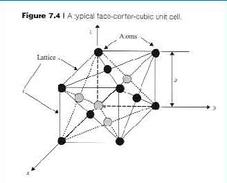 One of the first methods to create mono-crystalline silicon is by dipping a seed crystal in a bath of molten silicon. The atoms in the silicon attach to the seed crystal and pull it up from the bath, creating a boule. This is then carefully cut into wafers. The process of growing these materials can be done in a variety of ways. For example, it can be annealed and cooled, which makes it suitable for various applications.
Another method to manufacture single-crystalline silicon is by forming mono-crystalline silicon in a quartz crucible. This method is known as Czochralski growth, and it involves placing a seed crystal into a molten silicon bath. The atoms of silicon in the silicon melt attach to the seed crystal. The silicon melt is then drawn upward from the crucible, forming a boule. Once the boule has grown to the required size, it is carefully sliced into wafers.
Monocrystalline silicon does not have grains nor domains; it is monolithic.
However, it is not isotropic. Its Young modulus is different in different crystallographic directions. The strength is also different in different crystallographic directions. See below for more.
Lapped or Alkaline etched Silicon Wafer surfaces scatter light. Polished Silicon wafers are excellent reflectors of both visible and IR light. They are used for astronomic mirrors, for laser scanners and for controlled microscopic mirror arrays.
What are The Mechanical Properties of Monocrystalline Silicon?
A scientist asked us the following:
I also need to know how good the surface polish is over a 25mm diameter section in the dead center of the wafer in static situ? I am interested in the fineness of the grind and the flatness? Is their any grain to a wafer?
Thermal conduction properties are needed also. The end product would be a flexible reflector.
If my idea is correct it will generate a new manufacturing stream for you.
Below are the mechanical properties of monocrystalline silicon. Please send us any question.
| PROPERTY |
VALUE |
UNITS |
| Bulk modulus of elasticity |
9.8·1011 |
dyn/cm2 |
| Density |
2.329 |
g/cm3 |
| Silicon Hardness |
7 |
on the Mohs scale |
| Surface microhardness (using Knoop's pyramid test) |
1150 |
kg/mm2 |
| Elastic constants |
C11 = 16.60·1011 |
dyn/cm2 |
| C12 = 6.40·1011 |
dyn/cm2 |
| C44 = 7.96·1011 |
dyn/cm2 |
| Silicon Young's Modulus (E) |
[100] |
129.5 |
GPa |
| [110] |
168 |
GPa |
| [111] |
186.5 |
GPa |
| Shear Modulus |
64.1 |
GPa |
| Poisson's Ratio |
0.22 to 0.28 |
- |
Compressive Strength 960 MPa
Tensile Strength 350 MPa
Shear Strength 240 MPa
Thermal Expansion Coefficient 2.6E-6 /ºC
Thermal Conductivity 149 W/m/ºC
 Note that Silicon wafers are made from monocrystalline Silicon.
Such material does not have grains nor domains; it is monolithic.
However, it is not isotropic. Its Young modulus is different in different crystallographic directions.
The strength is also different in different crystallographic directions.
A silicon wafer when bent will break along cleavage planes.
A (100) Ori wafer will break into rectangular pieces, that is into pieces with 90º angles..
A (111) Ori wafer will break into pieces with 60º angles.
A (110) Ori wafer will break into pieces with 70.5 and 109,5º angles.
The compressive, tensile and shear strengths listed are bulk values.
In monocrystalline materials they are different in different directions
Standard 4"Ø wafers have total thickness variation of <10µm. Flatness, as measured by TIR is normally <7µm and central 25mm diameter area probably has TTV <2.5µm. Specially made 4"Ø wafers can have TTV<5 or even <1µm with TIR and TTV of central 25mm diameter, proportionally smaller.
Standard lapped or fine diamond ground 4"Ø wafers have TTV<4µm (which after polishing degrades to TTV<10µm) and Surface Roughness of about 50µm.
Standard polished 4"Ø wafers have TTV<10µm but Surface Roughnss <0.5nm as measured by an Atomic Force Balance over 2×2µm area {polishing a lapped wafer degrades its TTV some but improves Surface Roughness a lot}.
What Is the Yield Strength of Silicon?
What is the yield strength of silicon? It is a tetravalent metalloid and a hard, crystalline solid. 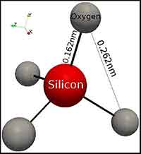 Its properties are described by its ultimate tensile strength, yield stress, and shear modulus of elasticity. This strength is an important parameter when designing structures and machines. The higher the yield stress, the stronger the material is. A semiconductor has a high yield stress because it resists bending under pressure.
Silicon has a high scratch hardness of about N/A. This measure of resistance to permanent plastic deformation is very useful in engineering applications. Its crystal structure is face-centered diamond-cubic. It has a relatively small Vickers hardness. It also has a low scratch hardness. These tests are important in the semiconductor industry, because silicon's hardness determines its ability to be cut into thin layers.
In mineralogy, this number is known as the Mohs hardness. It indicates the resistance of a material to permanent deformation. The hardness of silicon is measured using a scale called the Mohs hardness. The hardest mineral is diamond. It has a Mohs hardness of 7. In addition, its chemical composition and surface area are largely similar to diamond. This means that a semiconductor made from silicon is likely to be very hard.
The Mohs hardness of silicon is approximately N/A. This measure measures the resistance of a material to permanent plastic deformation. The hardness of silicon is determined by the Mohs scale. The harder the mineral, the higher its scratch hardness. A face-centered diamond-cubic crystal is the most common crystal structure of silicon. Its Vickers hardness is about N/A. The Mohs hardness is a qualitative test that can be used in mineralogy.
The yield strength of silicon is an important property in semiconductor manufacturing. Having a high yield of silicon means that it is easy to produce thin-films with high-quality components. However, it does not yield a high-quality semiconductor. This is a crucial factor for high-quality products. If you want to manufacture the perfect product, the yield strength of silicon is vital. It is a good choice for a variety of technical products.
The yield strength of silicon is determined by the mohs scale. It is the mechanical property of silicon. It is the most commonly used material in electronics. It is used in computers, televisions, and many other products. For example, it is used in smartphones. It is important to have a high yield strength in electronics. It is also necessary to use a strong binder. This will make the semiconductor more durable.
In electronics manufacturing, the yield strength is measured in terms of its ability to withstand forces without breaking or cracking. The yield strength is a function of the atoms' ability to resist the forces that can be applied to the material. In electronics manufacturing, the strain of Silicon is a critical parameter for a semiconductor. A large strain will result in a high level of friction and failure. Then, it is necessary to calculate the stress.
In electronics, the yield strength is the yield strength minus the stress. Its elastic properties are measured using the Young's modulus. Its flexibility can be measured by the stress-strain curve. The elastic properties of Silicon can be evaluated by measuring its flexibility. The mechanical properties of the silicon can be evaluated by determining its hardness and elastic resistance. For instance, the mechanical performance of the polysilicon is a factor that determines its yield. The yield is the amount of material it can handle before breaking or crumbling.
The yield strength of silicon is a measure of the material's elasticity. A high degree of stiffness indicates that the material will be able to withstand a force. If it breaks, the strength of silicon is an important factor. Its strength is directly related to the tensile strength of silicon. When it breaks, the stress is a measurement of its flexibility. When a semiconductor is cracked, it can be cracked. This is how a chip can be broken.
What is Silicon Hardness?
The Mohs scale of mineral hardness determines the resistance of a material to permanent plastic deformation. In general, the harder the material, the lower its scratch hardness. Silicon, which has a face-centered diamond-cubic crystal structure, is N/A on the Mohs scale. The Mohs scale is a qualitative measure of material hardness and is useful in mineralogy. Here, we will discuss the properties of silicon.
Its thermal stability has been studied by Ge, D., and Dominich, V. (1998). In the same journal, Gerk, A.P., and Tabor (1978) studied indentation hardness and structural relaxation in pure amorphous silicon. Phys. Rev. B 78, 224118, also reported a study of pressure-induced phase transitions in silicon. Another study, by Ruffell and Bradby, compared the hardness of amorphous and crystalline silicon under high pressure.
The yield strength of silicon is a fundamental property that can help determine the quality of semiconductors. Its high yield strength makes it easy to manufacture thin films containing high-quality components. Moreover, this material's elasticity can be evaluated using a stress-strain curve. The yield strength of silicon is a critical parameter for semiconductors, as a high yield strength makes semiconductors more durable. And this is just one of the reasons why silicon is a valuable material in the field of electronics.
When cutting silicon components, it is important to understand the underlying mechanism for how these processes impact the material's ductility. While the surface of silicon is smooth, the interior contains polycrystalline material and dislocations or microcracks. A few recent studies have revealed that mechanical machining processes alter silicon's ductility, affecting their optical and electrical properties. As a result, it is vital to understand the effects of mechanical machining on silicon hardness.
What is the Roughness Data on Monocrystalline Silicon Wafers
Rearcher question:
Do you have the roughness data on the quoted monocrystalline silicon wafers?
Item Qty. Description
EQ20b. 25/50/100 Silicon wafers, per SEMI Prime, P/E 2"Ø×1,000±25µm,
n-type Si:P[100]±0.5°, Ro=(1-50)Ohmcm, TTV<5µm,
One-side-polished, back-side Alkaline etched, SEMI Flat (one),
Sealed in hard cassette
UniversityWafer, Quoted and Replied. Reference #223840.
The offered Monocrystalline Silicon wafers are polished by the Semiconductor Industry Standard CMP (Chemical-Mechanical Planarization) process that usually yields Surface Roughness <1.0nm RMS as measured by AFB/AFM. However, this measurement is only done occasionally, and it is not a standard QC measurement done on each batch of wafers, so it is not reported in the Certificate of Conformance.

 One of the first methods to create mono-crystalline silicon is by dipping a seed crystal in a bath of molten silicon. The atoms in the silicon attach to the seed crystal and pull it up from the bath, creating a boule. This is then carefully cut into wafers. The process of growing these materials can be done in a variety of ways. For example, it can be annealed and cooled, which makes it suitable for various applications.
 Note that Silicon wafers are made from monocrystalline Silicon.