
Hello I'm looking for a 32mm diameter zero-background holder for XRD applications. The plate should have a 10-15 mm diameter cavity with a depth of < 500 micrometers. Is this something I can purchase from your company?
Researching Silicon Pocket Wafers
A postdoc requested a quote for the following:
UniversityWafer, Inc. Quoted
Item Qty. Description
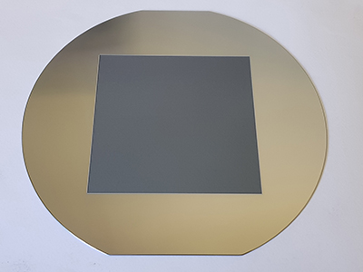
HD38n. 5/10 Zero Diffraction Plate for XRD with pocket
Material: CZ Silicon, Diameter: 32.0±0.3 mm
Thickness: 2000±50 µm
Type/Dopant: P/Boron
Resistivity: >10 Ohm-cm
Surfaces: Single side polished / etched
Flats: none
Edge rounding: straight
Central pocket: Diameter: 12.5±1.5 mm
Depth: ~200 µm,
CTQ: Adequately oriented to guarantee zero background.
Please reference # 271035 for pricing/lead time.
Get Your Quote FAST! Or, Buy Onlineand Start Researching Today!
Why Was Silicon Pocket Wafers Developed?
The Silicon Pocket Wafer was developed by MIT engineers, who used it to meet their specific semiconductor fabrication requirements. The pocket wafer can be used to enable chip manufacturers to prototype work with silicon ever smaller transistors, as well as provide custom designs for silicon and other materials. It also allows existing wafers to be reused, and nonepitaxial single crystalline growth can be achieved using a SEM. This method is faster than other existing methods for meeting development specifications, and it allows for the fabrication of ever smaller transistors in less time.
Related Silicon Materials
- Silicon Wafers
- Silicon Wafer Diameters
- Zero Background Sample Holders
- SOI Wafers
- MEMS Wafers
- Thermal Oxide Silicon Wafers
What is a Silicon Pocket Wafer?
A silicon pocket wafer used to fabricate microelectronic devices. A silicon pocket wafer is called so because it  has shallow "pockets" etched into the surface. These pockets are used to isolate individual devices on the wafer and to protect them during subsequent processing steps. The etched pockets also allows the wafers to be diced into individual die Integrated Circuits (ICs) after the processing, which can then be packaged and used in electronic devices.
Pocket Wafer Used in Metrology Equipment
An semiconductor equipment technician requested the following quote:
I am looking for a 200mm carrier wafer with a 100mm pocket in the center. This carrier wafer will be used to transport a 100mm wafer in metrology equipment. Do you have anything like this? If not would you be able to direct me to someone who may?
UniversityWafer, Inc. Quoted:
200mm carrier wafer with a 100mm pocket in the center.the pocket depth ~300um, This carrier wafer will be used to transport a 100mm wafer in metrology equipment. Qty. 5 and 25
Reference #142962 for specs and pricing.
What are Silicon Pocket Wafer Applications?
Silicon Pocket Wafer is the industry standard for silicon wafers used in photovoltaics, semiconductors, and MEMS semiconductor industries. They are available in different wafer diameters from 50mm to 200mm and can be used for solar cells or other photovoltaics. The use of silicate wafers enables engineers to create 2D materials and transition the electronics industry from traditional to fully tailored process designs with higher performance materials. Glassware managed manufacturing processes are also available with Silicon Pocket Wafer, making it ideal for scientists, SEM, SC and other equipment that require a specific diameter. It is commonly used in the production of solar cells and mm sized equipment that require precision control during processing.
Pocket Carrier Wafer to use in HDPCVD System
A postdoc requested the following quote:
I wanted to pick your brain on if you had something that would make sense for me in terms of a pocket carrier wafer. What I’m looking for is just a boring old 4” si carrier to use in our HDPCVD system which would hold student sample pieces. We don’t really use any crystalbond on the carriers since it would melt at the 150-170C we’re using. The pieces have a tendance to slide around during loading and get pinched in the tool, causing all kinds of issues. We of course could just make our own etched pocket wafers, but I don’t really have the logistics to do this in quantities of 50-100 which is what I’d like to keep on hand. I figure that would last me a couple years. Is this something that would make any kind of sense to pursue with you?
Trying to stay under 5k, basically we’re trying to figure out whether we can do this efficiently in bulk or if we should just push the pocket wafer etching onto the students. I didn’t really know what sort of options were available for medium-size batch etching; I know it’s a fair amount of work to have someone etch them singly, so I understand why it’s expensive even with a laser etcher. I appreciate your time on this.
Drawing is attached.
We have a laser machine and we need the following info.
- What depth of the pocket would you like?
- How many pocket-wafers are needed?
- Is R50.00 the radius of the wafer?
- Do you have any requirements for the carrier wafer, like thickness, doping level, polishing etc?
I attach pictures from previous work.
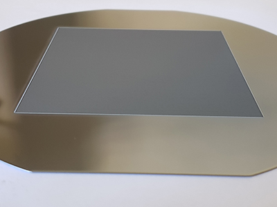
UniversityWafer, Inc. quoted the following. Reference #265082 for pricing.
Item Qty. Description HQ33b. 100 Silicon wafers, per SEMI Prime, P/E 4" (100.0±0.5mm)Ø×525±25µm, With 40x40mm recessed squares in the center, 200 microns deep, Type/dopant: p/B, Resistivity: >1 Ohm-cm, Orientation: [100]±0.5°, One-side-polished, back-side etched, Polished side with the pocket, Pocket side aligned to primary flat, SEMI Flat (one): 32.5±2.5mm, Back side laser mark: present, Sealed in Empak or equivalent cassette, Note: See HQ33b drawing for details.
