
“I need PECVD silicon nitride to use for membranes and cantilevers. Thermal conductivity of this film is important in my project. Would you please send me the thermal conductivity of your low-stress PECVD silicon nitride? I also wonder how you can control it.”
Silicon Nitride Membranes and Thermal Conductivity
Silicon wafers coated with silicon nitride (SiNx) are widely used to fabricate suspended membranes, cantilevers, microheaters, thermal sensors, MEMS devices, and other micro- and nanoscale structures. In these applications, understanding both the thermal properties of the silicon substrate and the deposited silicon nitride film can be important for predicting heat flow, temperature gradients, and thermal stress.
A researcher requested silicon wafers with low-stress PECVD silicon nitride for membrane and cantilever fabrication and specifically asked about the thermal conductivity of the deposited film:
Example Low-Stress PECVD Silicon Nitride Wafer
UniversityWafer, Inc. quoted:
Item FA46 — Quantity: 10
100 mm (4 inch) silicon wafers, SEMI Prime, 525 ± 25 µm thick,
single SEMI flat, p-type boron-doped Si (100) ± 0.5°,
resistivity 5–10 Ω·cm, TTV < 4 µm, bow < 12 µm,
warp < 30 µm, with approximately 1.0 µm of
low-stress PECVD silicon nitride on the polished side.
Reference #225415 for specifications and pricing.
Thermal Conductivity of Silicon Nitride Thin Films
The thermal conductivity of deposited silicon nitride should not be treated as one universal material constant. Unlike high-quality crystalline silicon, PECVD silicon nitride is typically amorphous or structurally disordered, and its thermal properties can depend strongly on film composition, density, hydrogen content, deposition conditions, thickness, and post-deposition processing.
Consequently, the thermal conductivity of a specific PECVD SiNx film may differ substantially from values reported for bulk or crystalline silicon nitride. Researchers performing quantitative thermal modeling should therefore use film-specific measurements or process-specific data whenever possible rather than assuming a bulk silicon nitride value.
Why Low-Stress Silicon Nitride Is Used for Membranes
Residual film stress is especially important when silicon nitride is used to fabricate suspended structures. Excessive tensile or compressive stress can influence membrane flatness, mechanical behavior, dimensional stability, and device yield.
Low-stress films are therefore useful for applications such as MEMS membranes, cantilevers, microbridges, sensor platforms, microheaters, and suspended thermal structures.
UniversityWafer can provide silicon substrates with PECVD silicon nitride for research and device-development applications.
Heat Flow Through Silicon and Silicon Nitride
In a silicon wafer carrying a thin silicon nitride layer, heat can move through several different pathways. Bulk crystalline silicon generally provides a relatively effective heat-conduction path, while a suspended silicon nitride membrane can provide much greater thermal resistance because of its thin geometry and lower thermal conductivity.
This difference can be deliberately exploited in MEMS devices. Removing the silicon beneath selected regions can create suspended membranes that reduce heat loss into the substrate. The resulting thermal isolation is useful when a device must reach or detect a temperature different from the surrounding wafer.
Applications of Silicon Nitride Membranes
Silicon nitride films on silicon substrates are used in research involving:
- MEMS membranes and cantilevers
- Microheaters and thermal sensors
- Bolometers and infrared detectors
- Calorimetric sensors
- Suspended microstructures
- Microfluidic heating platforms
- Thin-film thermal conductivity measurements
- Electron and X-ray transparent membrane windows
- Nanofabrication and materials characterization
Silicon Thermal Conductivity in MEMS Design
The silicon substrate itself also plays an important role in device thermal behavior. Near room temperature, high-quality crystalline silicon has a thermal conductivity on the order of 150 W/m·K, although the exact value depends on temperature, doping, impurities, crystal quality, and dimensions.
As temperature increases above room temperature, the thermal conductivity of crystalline silicon generally decreases because phonon-phonon scattering becomes stronger. Heavy doping, defects, interfaces, and reduced dimensions can further influence heat transport.
These effects should be considered when modeling devices in which heat travels from a silicon nitride membrane into a silicon wafer substrate .
Thermal Expansion and Thin-Film Stress
Thermal conductivity is not the only thermal property that matters in a silicon/SiNx structure. Differences in the coefficient of thermal expansion (CTE) between the silicon substrate and deposited films can generate mechanical stress during heating and cooling.
This becomes particularly important during deposition, annealing, thermal cycling, and high-temperature device operation. Film thickness, intrinsic deposition stress, temperature history, and membrane geometry should therefore be considered together when designing suspended structures.
Selecting Wafers for Thermal and MEMS Research
Researchers designing thermal MEMS structures should consider several substrate specifications, including wafer thickness, crystal orientation, resistivity, doping, surface finish, film thickness, and film stress. These parameters can affect both fabrication and final device performance.
For membrane fabrication, Si (100) substrates are commonly used when crystallographic wet etching is part of the process because anisotropic silicon etchants can produce well-defined structures determined by the crystal planes. The appropriate substrate ultimately depends on the device geometry and fabrication process.
UniversityWafer supplies silicon wafers and deposited thin-film substrates for MEMS, semiconductor, microfabrication, thermal transport, and materials-science research.
Get Your Silicon Wafer Quote FAST!
Or,
Buy Wafers Online
and Start Researching Today!
Thermal Properties of Silicon Wafers
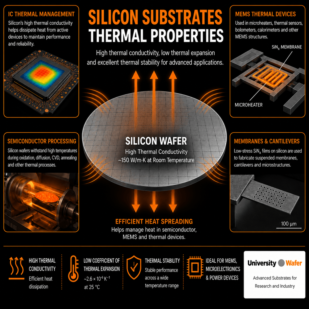
The thermal properties of silicon are important in semiconductor fabrication, MEMS, integrated circuits, sensors, power electronics, and other applications where silicon wafers experience heating or repeated temperature cycling. Important parameters include thermal conductivity, coefficient of thermal expansion (CTE), heat capacity, and the dependence of these properties on temperature, crystal quality, and doping.
Near room temperature, high-quality crystalline silicon has a thermal conductivity of approximately 150 W/m·K, although the exact value depends on temperature, impurity concentration, isotope composition, and crystal quality. This relatively high thermal conductivity helps silicon spread heat generated by electronic devices across the wafer and toward the package or heat-removal structure.
Why Silicon Thermal Conductivity Matters
Thermal conductivity describes how efficiently heat is transported through a material. In crystalline silicon, heat is carried primarily by lattice vibrations called phonons. Phonon scattering limits thermal transport and can be influenced by temperature, impurities, defects, interfaces, and nanoscale dimensions.
Thermal management becomes increasingly important as device dimensions decrease and power density increases. Excessive local heating can change transistor characteristics, accelerate material degradation, alter carrier mobility, and create mechanical stress between materials with different thermal expansion coefficients.
Researchers developing semiconductor devices can select silicon wafers according to diameter, thickness, crystal orientation, conductivity type, dopant, resistivity, and surface finish.
Temperature Dependence of Silicon Thermal Conductivity
The thermal conductivity of crystalline silicon is strongly temperature dependent. Around and above room temperature, thermal conductivity generally decreases as temperature rises because phonon-phonon scattering becomes stronger.
For this reason, a single room-temperature thermal conductivity value should not be used for every semiconductor thermal simulation. Device designers working across a wide temperature range should use temperature-dependent material data appropriate for the silicon grade and operating conditions being modeled.
Effect of Doping on Silicon Thermal Conductivity
Dopants such as boron, phosphorus, arsenic, and antimony are introduced into silicon to control its electrical resistivity and carrier concentration. At sufficiently high concentrations, dopant atoms can also increase phonon scattering and reduce thermal conductivity relative to high-purity crystalline silicon.
The effect becomes especially relevant in heavily doped device regions where both electrical and thermal properties must be considered. Thermal conductivity therefore depends not only on the silicon crystal itself but also on the material's impurity and defect concentrations.
Learn more about heavily doped silicon wafers for applications that require low electrical resistivity.
Coefficient of Thermal Expansion of Silicon
Silicon has a relatively low coefficient of thermal expansion. Near room temperature, its linear CTE is approximately 2.6 × 10⁻⁶ K-1, although the value changes with temperature.
CTE is especially important when silicon is bonded, coated, or packaged with other materials. If two materials expand at substantially different rates during heating, thermal cycling can generate mechanical stress at their interface.
This consideration is important in wafer bonding, thin-film deposition, MEMS structures, semiconductor packaging, and multilayer devices containing materials such as silicon dioxide, silicon nitride, metals, glass, sapphire, or compound semiconductors.
Thermal Stress During Semiconductor Processing
Silicon wafers routinely experience elevated temperatures during thermal oxidation, diffusion, annealing, chemical vapor deposition (CVD), and other semiconductor fabrication processes. Temperature gradients across a wafer can produce nonuniform thermal expansion and mechanical stress.
Wafer thickness, diameter, crystal quality, film stress, heating rate, cooling rate, and the properties of deposited layers all influence how a wafer responds to a thermal process. Proper temperature control helps reduce wafer bow, film cracking, delamination, and other process-related problems.
Silicon Thermal Properties in Integrated Circuits
Integrated circuits generate heat whenever electrical power is dissipated within transistors, interconnects, and other device structures. Silicon conducts part of this heat through the substrate toward the backside of the die and ultimately into the package and cooling system.
As transistor density and device power density increase, localized hot spots can form. Accurate thermal modeling is therefore important for predicting junction temperatures, improving reliability, and designing effective heat-removal pathways.
Silicon Wafers for MEMS Thermal Devices
Silicon's combination of thermal, mechanical, and microfabrication properties also makes it useful for MEMS thermal devices. Silicon substrates are used in microheaters, thermal sensors, bolometers, calorimeters, microfluidic heaters, temperature sensors, and other microsystems.
MEMS designers may use bulk silicon, thin silicon membranes, or silicon-on-insulator (SOI) wafers depending on the desired thermal isolation, structural thickness, and fabrication process.
Bulk Silicon vs. Thin Silicon Structures
Thermal behavior changes as silicon dimensions become smaller. Bulk crystalline silicon can conduct heat efficiently, while very thin silicon layers, nanostructures, and patterned membranes may exhibit substantially lower effective thermal conductivity because phonons interact more frequently with surfaces and interfaces.
This size-dependent behavior is important in nanoscale electronics, MEMS membranes, silicon photonics, thermoelectric research, and other devices where the dimensions of the silicon structure approach relevant phonon transport length scales.
Applications That Depend on Silicon Thermal Properties
Understanding silicon thermal behavior is useful when selecting substrates for applications including:
- Integrated circuits and CMOS research
- Power semiconductor devices
- MEMS sensors and actuators
- Microheaters and thermal sensors
- Silicon photonics
- Wafer bonding experiments
- Thermal oxidation and diffusion studies
- Thin-film deposition research
- Microfluidic heating devices
- Thermal conductivity and heat-transfer experiments
Selecting Silicon Wafers for Thermal Research
The appropriate silicon substrate depends on the thermal experiment or device being developed. Researchers should consider wafer diameter, thickness, crystal orientation, doping level, electrical resistivity, growth method, and surface finish.
Czochralski (CZ) and Float-Zone (FZ) silicon can have different impurity concentrations, particularly oxygen content, which may be relevant in experiments requiring highly controlled electrical or thermal material properties.
UniversityWafer supplies monocrystalline silicon wafers for semiconductor fabrication, MEMS, thermal research, microelectronics, photonics, and materials-science applications.
Related Silicon Wafer Resources
Explore related silicon substrates, thin-film technologies, and semiconductor processes used in thermal research, MEMS, and microfabrication.
- Silicon Wafers – Explore monocrystalline silicon substrates for semiconductor, MEMS, photonics, and materials research.
- Heavily Doped Silicon Wafers – Learn how high dopant concentrations influence silicon wafer electrical and material properties.
- PECVD Silicon Nitride – Silicon wafers with deposited silicon nitride films for MEMS, membranes, cantilevers, and microfabrication.
- Silicon Nitride (SiNₓ) – Learn about silicon nitride thin films and their applications in semiconductor and MEMS structures.
- Microfabrication – Learn about wafer-based fabrication processes used to create microscale semiconductor and MEMS structures.
- Thermal Oxide on Silicon – Explore silicon dioxide layers thermally grown on silicon substrates for device fabrication and research.
- Silicon Wafer Dicing – Learn about cutting silicon wafers into dies and custom substrate dimensions for research and device fabrication.