Fabricating Nanostructures by Electron Beam Lithography
A nanotechnology researcher requested the following quote:
We are working on nanostructures made of silicon. Usually, the thickness of silicon film ranges from 300nm to 700nm in our research. The substrate can be SiO2 or other transparent insulators. Do you think it is possible to provide silicon film at this thickness range?
We need Si film with thickness ranging from 300 nm to 700 nm on a transparent substrate. Crystalline or amorphous silicon?
The extinction efficiency is quite important for us. Could you please provide the refractive index and extinction efficiency to us?
We will use SOI to fabricate nanostructures by electron beam lithography. The SOI should be transparent. The absorption of Si should be as small ad possible.
Reference #205719 for specs and pricing.
Get Your Quote FAST! Or, Buy Online and Start Researching Today!
Photolithography Prepared Micro-Electrodes
Researcher Request:
We are in requirement of Photolithographically prepared microelectrodes (Cr/Au) (Design we will provide with minimum feature size 3 micron ) on Si/SiO2 wafer Cr/Au Design:
Will provide later if agrees (Min. feature size 3micron) Silicon wafer details: Diameter: 4” (100 mm) Type: P type Dopant: Boron Orientation: <100> Resistivity: 1 to 20 Ωcm Thickness: 500 μm SiO2 Thickness: 100 nm (Single side coating) Surface: One Side Polished I would be highly obliged if you could kindly provide the above.
UniversityWafer, Inc. Replied:
Photolithographically prepared microelectrodes (Cr/Au) (Design we will provide with minimum feature size 3 micron ) on Si/SiO2 wafer Cr/Au Design: Will provide later if agrees (Min. feature size 0.18micron) Silicon wafer details: Diameter: 6” (150 mm) Type: P type Dopant: Boron Orientation: <100> Resistivity: 1 to 20 Ωcm Thickness: 500 or 675 μm SiO2 Thickness: 100 nm (Single side coating) Surface: One Side Polished
Design: Electrode-Final - Design
Please reference #265449 for quote.
Substrates for Lithography Debugging
A electrical engineer requested a quote for the following:
Pls check if you have 25pcs each below wafer?
6 inches SI bare wafer, 0.1µm TTV and 0.5µm TTV, Standard thickness, Application: Lithography debugging. Could you offer <0.1um TTV and < 0.5um TTV?
UniversityWafer, Inc. Quoted:
Substrate Description
Silicon wafers, per SEMI Prime, P/P 6"Ø×750±25µm,
n-type Si:P[100]±0.5°, Ro=(1-100)Ohmcm,
TTV<0.5µm,
Both-sides-polished, One SEMI Flat (57.5mm),
With Lasermark.
With Final Polish (TTV measured before final polish).
Reference RFQ#211437 for specs and pricing.
Related Lithography and Wafer Fabrication Resources
A Brief Overview of Lithography in Engineering
Lithography is a basic fabrication technique used in the manufacture of semiconductor devices. It is a crucial process in manufacturing integrated circuits and micro-nonfabrication technologies. This book explores the principles and processes of lithography and the materials that are used in the process. This book provides an overview of lithography as a fundamental fabrication process in engineering. It is useful for anyone interested in microscopic structures.
Lithography is a process of creating nanometer-sized structures. The lithographic process involves drawing a design on a flat stone or metal plate, and then chemically affixed it to the surface. This is an important step in the manufacturing process, because it allows for a variety of designs and patterns. The most common application of lithography is to print electronic circuit boards. The process is also used to create printed circuit boards.
Photolithography, also known as UV lithography, is a method of microfabrication in which an image is transferred onto a light-sensitive chemical photoresist. After the artist is satisfied with the image, the lithograph is treated with a chemical etch. Then, the printed part is rolled up or washed out. This process allows the lithograph to be reused.
During the lithographic process, a drawing is drawn onto a flat stone or metal plate using a special greasy pencil. The drawing material is then chemically etched once the artist is satisfied with the design. After the artist is satisfied with the result, the image is removed and the printing element can be reused. Washing and rolling the lithograph is the final step in reusing it.
Lithography is a planographic printing process that allows for the replication of nanometer-scale structures. The drawing material is made using a special greasy pencil or litho crayon. After the artist has satisfied the image, the lithograph is treated with a chemical etch. Finally, the lithograph is re-graining the stone to remove the greasy image and reuse it again.
In general, lithography is used to produce nanometer-scale structures. This process involves the use of specialized greasy pencils or litho crayons to replicate a pattern into a substrate. The image is subsequently chemically etched. This process produces images that are highly accurate. This paper is a perfect example of a lithographic printing. A lithograph is the most effective method for replicating a design.
Lithography is a process that reproduces images onto a substrate. The process of lithography involves the use of a greasy pencil to draw an image, or a flat stone. The drawing is made on the printing element, such as paper or glass. After the image is created, the printed material is chemically etched to remove the greasy image. The resulting picture is called a lithograph.
The process of lithography is a process that creates nanometer-sized structures. The greasy pencil is used to draw the image on the printing element. The greasy pencil is then transferred onto the surface of the substrate with the help of a chemical. Once the artist is satisfied with the results, the greasy drawing is transferred to the printing element. The resulting image is then etched with a chemical.
The process of lithography is the fabrication of nanometer-sized structures. The process uses a greasy pencil or a flat stone to draw an image. Then, it requires chemical etching to remove the image. The resulting images are then transferred to a new material. There are many benefits to lithography. For instance, it can be used to print high-quality 3D printed images.
Lithography uses different processes to produce patterned films on a surface. The first stage of lithography is exposing a surface to light. The second stage involves the removal of the light-sensitive coating. The process is called photolithography. The first step is similar to etching. The final step of photolithography is the printing of the image. The next stage is the cutting of the printed image.
Video Photolithography Defined
What Substrates Can Be Used for Soft Lithography?
A biomedical engineer requested the followng quote:
I'd like to receive a quote so
we can place an order on 25 x
3" silicon wafers with the
following specifications: 76.2mm
N/PH <1-0-0> 1-10OHM-CM,
381+/-25um prime wafer; single
side polished, 2 semi standard
flats.
We received the order for silicon item #695; thanks for all your help. The wafers are great quality. We use them for soft-lithography, which we use to fabricate
microfluidic devices.
Reference #211786 for specs and pricing.
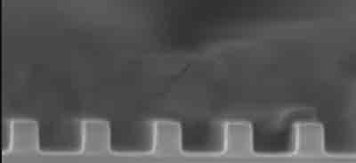
Researcher Uses Lithography to Make Pattern on Un-Patterned Silicon Wafers
A solid mechanics Ph.D. student requested a quote for the following:
I want to buy some patterned silicon wafer. The pattern is the line pattern with width smaller than 500 nm. Do you have this kind of product? Or I need to use lithography to get this pattern based on the un-patterned silicon wafer?
I have already bought the silicon wafer 444 for many times. Recently I order some more silicon wafer on you website. I usually use them as the substrate for the graphene under AFM observations. Now I hope there are periodic gratings (i.e. <=500 nm) on the wafer surface. If you have this kind of product, it will be much helpful. Otherwise, I have to do the lithography and get this kind of pattern by myself.
The grating I want is like the following. The surface of the silicon wafer is not flat. Instead, there is periodic grating on its surface. The width of the groove is less than 500nm.
UniversityWafer, Inc. Questions:
I think we can offer you a patterned wafer with feature size below 500nm. In your pictures I could see also dimensions down to 70nm. This is quite tricky for us because we have only 130nm capability.
We need detailed specification to determine initial costs for the project and costs per wafer.
[Q1] Can you give us more details regarding your request?
[Q2] What kind of pattern do you need?
[Q3] Which dimensions and tolerances?
[Q4] Depth of structures?
[Q5] How many wafers do you need and how often?
At this feature size we have mask reticles which we step over the wafer. Per reticle CD structures are necessary. I hope this is not a problem.
Best regards and looking forward for your specifications
Researcher Answer:
A1: In our experiment, we need the period of the feature less than 200nm. (i.e. ridge width + valley width <= 200 nm)
A2: Currently, periodic line pattern is enough for initial study.
A3: Dimension of the wafer should be at least 10mm * 10mm.
A4: Depth of the pattern is not important. 10nm ~ 100 nm is good.
A5: It depends on the price and the quality of the wafer. For the initial experiment, we don't need much (may be around 10). After successful attempt, we may need much more.
Reference #250898 for specs and pricing.
