Request a Quote for Silicon Wafers
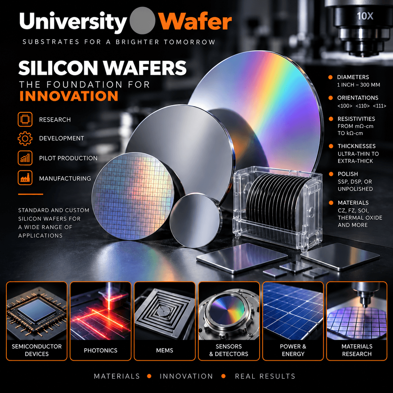
UniversityWafer supplies silicon wafers (Si) for semiconductor fabrication, MEMS, photonics, sensors, power electronics, university research, and prototype development. We offer prime, test, mechanical, float zone (FZ), Czochralski (CZ), SOI, and oxide-coated silicon wafers in diameters from 25 mm to 300 mm.
Request custom wafer specifications including diameter, crystal orientation, dopant, resistivity, thickness, polish, oxide or nitride coatings, and quantity. Our technical team will provide a fast quotation for research or production requirements.
Get Your Silicon Wafer Quote FAST! Or, Buy Online and Start Researching Today!
Silicon Wafer Inventory
- Prime Grade Silicon Wafers
- Test Grade Silicon Wafers
- Mechanical Grade Silicon Wafers
- Float Zone (FZ) Silicon
- Czochralski (CZ) Silicon
- Silicon-on-Insulator (SOI) Wafers
- Thermal Oxide Silicon Wafers
- Silicon Nitride Coated Wafers
- Undoped and Doped Silicon
- Single- and Double-Side Polished Wafers
- High-Resistivity Silicon
- Ultra-Thin and Thick Silicon Wafers
- Partial Cassettes and Custom Wafer Sizes
We maintain inventory for immediate shipment and can also manufacture custom silicon wafers to your exact specifications for semiconductor, MEMS, photonics, and advanced materials research.
Silicon Wafer Inventory for Research and Production
UniversityWafer supplies silicon wafers for research, prototyping, process development, pilot production, and semiconductor manufacturing. Available materials include prime grade, test grade, mechanical grade, Czochralski (CZ), Float Zone (FZ), silicon-on-insulator (SOI), thermal oxide, and other coated or processed silicon substrates.
Silicon wafers are available in a wide range of diameters, thicknesses, crystal orientations, resistivities, dopants, and surface finishes. Researchers can source both standard inventory and custom specifications for applications in MEMS, photonics, RF, sensors, power electronics, microfabrication, semiconductor processing, and materials research.
Featured Silicon Wafer Options
High-Resistivity Float Zone Silicon
Float Zone (FZ) silicon is produced without a quartz crucible during crystal growth, which generally results in lower oxygen concentration than conventional CZ silicon. High-resistivity FZ material is frequently selected for applications where low free-carrier absorption, reduced substrate conductivity, or high material purity is important.
Common research applications include:
- RF and microwave devices
- Terahertz research
- Photonics and infrared research
- Radiation and particle detectors
- High-voltage and power devices
- Semiconductor characterization
High-resistivity FZ silicon may be available with resistivities extending into the kΩ-cm range, depending on diameter, orientation, conductivity type, thickness, and inventory.
Silicon-on-Insulator (SOI) Wafers
Silicon-on-insulator wafers consist of a thin silicon device layer separated from a silicon handle wafer by a buried oxide layer (BOX). SOI is widely used in silicon photonics, MEMS, CMOS research, sensors, RF devices, waveguides, and advanced semiconductor structures.
Important SOI specifications include:
- Device-layer thickness
- Buried oxide (BOX) thickness
- Device-layer resistivity
- Handle-wafer resistivity
- Crystal orientation
- Wafer diameter and total thickness
Thermal Oxide Silicon Wafers
Thermal oxide silicon wafers have a silicon dioxide (SiO2) layer grown by thermal oxidation of the silicon surface. Thermal oxide is widely used as an electrical insulator, dielectric layer, masking material, optical layer, and surface for device fabrication.
Available oxide specifications can include different oxide thicknesses, wafer diameters, conductivity types, resistivity ranges, and single- or double-side-polished substrates.
Ultra-Thin Silicon Wafers
Ultra-thin silicon wafers are useful when reduced substrate thickness, low mass, compact device geometry, or specialized mechanical behavior is required.
Applications can include:
- MEMS and microsystems
- Optical and photonic devices
- Sensor development
- Advanced packaging
- Temporary and permanent wafer bonding
- Flexible or mechanically compliant research structures
Very thin silicon requires careful handling because reduced thickness can increase susceptibility to bow, warpage, and mechanical breakage.
Silicon Wafer Grades
Prime Grade Silicon
Prime-grade wafers are intended for applications requiring tightly controlled surface quality and wafer specifications. They are commonly used for device fabrication, lithography, thin-film deposition, epitaxy, and semiconductor research.
Test Grade Silicon
Test-grade wafers are often used for process development, equipment testing, deposition trials, etching, cleaning studies, and laboratory experiments where full prime-grade specifications may not be necessary.
Mechanical Grade Silicon
Mechanical-grade silicon can be suitable for applications where the wafer is primarily used as a carrier, support substrate, handling wafer, dummy wafer, or mechanical component rather than as an active semiconductor device substrate.
Important Silicon Wafer Specifications
Selecting the correct silicon wafer requires more than choosing a diameter. The most important specification depends on the fabrication process and intended device.
- Diameter: From small research wafers to 300mm formats
- Crystal orientation: Common orientations include <100>, <110>, and <111>
- Conductivity type: P-type or N-type
- Dopant: Common dopants include boron, phosphorus, arsenic, and antimony
- Resistivity: Available across a wide range depending on material and growth method
- Thickness: Standard, ultra-thin, and extra-thick silicon options
- Surface finish: Single-side polished (SSP), double-side polished (DSP), or unpolished options depending on inventory
- TTV, bow, and warp: Important for precision processing, lithography, bonding, and optical applications
- Surface layers: Thermal oxide, silicon nitride, metals, and other deposited films may be available
Silicon Wafer Applications
Silicon remains one of the most widely used substrate materials in semiconductor and advanced materials research because of its mature fabrication infrastructure, well-characterized electrical properties, mechanical stability, and compatibility with many deposition, lithography, etching, oxidation, and bonding processes.
UniversityWafer silicon substrates support research involving:
- Integrated circuits and semiconductor devices
- MEMS and microfabrication
- Silicon photonics
- Optical sensors and detectors
- RF and microwave research
- Power electronics
- Thin-film deposition
- Nanotechnology
- Wafer bonding
- Solar and energy research