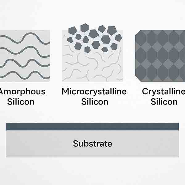
Amorphous and Microcrystalline Silicon Thin Film Solar Cells
A Ph.D. candidate requested a quote for the following.
I'm looking for a supplier of glass substrates (with TCO) for manufacturing of silicon thin film solar cells in our laboratory. Do you have in your offer such substrates (asahi, shott, other) ?
I would like to buy ~50 of glass substrates (dimensions 5x5 cm) for now, and few silicon, but I don't know if you have glass substrates for solar cells in your offer, or equivalents from other glass substrates manufacturers if you have such in your offer. This would be substrates for amorphous and microcrystalline silicon thin film solar cells.
Reference #156297 for specs and pricing.
Get Your Quote FAST! Or, Buy Online and Start Researching Today!
Silicon Wafers for use as the
Bottom Cell in Silicon Tandem Cells
A Ph.D research group leader requested a quote for the following.
I’m interested in supply of
silicon wafers for use as the
bottom cell in silicon tandem
cells. Our group investigates
perovskite materials and I’d
like to supply the silicon
wafer an fabricate the top cell
as a superstrate from a
perovskite stack.
The typical silicon bottom cell
structure is:
Do you have a product similar
to this? Do you supply wafers
to other groups for this
purpose?
Most likely we’ll need to cut-
down the wafer for research
scale cells. Any
recommendations on appropriate
wafer dimensions for such
purposes would be appreciated.
Reference #216974 for specs and pricing.
What is Microcrystalline Silicon?
Microcrystalline silicon (μc-Si or mc-Si) is a form of silicon that consists of small crystalline grains (nanometers to micrometers in size) embedded within an amorphous silicon matrix. It's considered a hybrid material because it exhibits properties of both amorphous silicon (a-Si) and crystalline silicon (c-Si).

🔬 Key Characteristics
-
Structure: Mixture of tiny silicon crystals (grains) and disordered amorphous regions.
-
Bandgap: ~1.1 eV, similar to crystalline silicon, making it suitable for electronic applications.
-
Mobility: Higher electron and hole mobility than amorphous silicon but lower than crystalline silicon.
-
Stability: More thermally and optically stable than amorphous silicon, especially under prolonged light exposure (reduced Staebler-Wronski effect).
⚙️ How It's Made
Microcrystalline silicon is typically deposited using plasma-enhanced chemical vapor deposition (PECVD) from a gas mixture of silane (SiH₄) and hydrogen (H₂). The hydrogen plays a crucial role in:
-
Promoting crystalline grain formation
-
Passivating dangling bonds
-
Controlling film structure
⚡ Applications
-
Solar Cells:
-
Thin-Film Transistors (TFTs):
-
Sensors:
-
Memory Devices:
📊 Advantages Over Amorphous Silicon
| Property |
Amorphous Silicon (a-Si) |
Microcrystalline Silicon (μc-Si) |
| Bandgap |
~1.7 eV |
~1.1 eV |
| Stability |
Degrades under light |
More stable |
| Mobility |
Low |
Higher |
| Efficiency (solar) |
Lower |
Higher in tandem devices |
Microcrystalline Silicon in Semiconductor Technology
Overview
Microcrystalline silicon (μc-Si:H) is a form of silicon characterized by small crystalline grains within an amorphous phase. This unique structure offers advantages over amorphous silicon, such as higher carrier mobility and enhanced stability, making it valuable in semiconductor applications.
Properties
- Structure: Comprises tiny crystalline grains embedded in an amorphous silicon matrix.
- Bandgap: Approximately 1.1 eV, similar to crystalline silicon, allowing for effective absorption of red and infrared light.
- Stability: Exhibits greater stability compared to amorphous silicon, attributed to its lower hydrogen concentration.
Applications
Microcrystalline silicon is widely used in various applications, including:
- Thin-Film Solar Cells: Serves as the bottom cell in tandem configurations, enhancing overall efficiency by absorbing longer wavelengths.
- Thin-Film Transistors (TFTs): Utilized in flat-panel displays due to its favorable electronic properties.
Advantages
- Enhanced Carrier Mobility: The presence of crystalline grains facilitates better charge transport.
- Improved Optical Absorption: Effective in absorbing red and infrared light, beneficial for photovoltaic applications. s.
