
Remote Epitaxy Wafers and Graphene Substrates
UniversityWafer, Inc. supplies substrates and research materials used in remote epitaxy, including graphene, silicon wafers, gallium arsenide (GaAs), and GaN templates. These materials support advanced semiconductor research involving reusable wafers, flexible electronics, and thin-film layer transfer.
Researchers at MIT demonstrated that an ultrathin graphene layer can enable remote epitaxial growth on crystalline substrates, allowing high-quality semiconductor films to be separated from the original wafer for reuse. This approach has the potential to reduce manufacturing costs while improving the scalability of advanced semiconductor devices.
UniversityWafer and its manufacturing partners can provide custom wafer pieces as well as 2-inch and larger GaN templates for remote epitaxy and related research projects.
Get your Remote Epitaxy quote FAST! Or, Buy Online and start researching today!
How Does Remote Epitaxy Work?
Remote epitaxy begins with a high-quality single-crystal wafer coated with an atomically thin graphene layer. Although graphene acts as a physical separation layer, the crystal potential of the underlying substrate can still guide the growth of a new epitaxial semiconductor film.
After growth, the epitaxial layer can be released from the graphene interface while leaving the expensive substrate largely undamaged. The original wafer may then be reused for additional growth cycles, significantly reducing substrate consumption and manufacturing costs.
Why Researchers Use Remote Epitaxy
Remote epitaxy is attracting interest because it combines high-quality epitaxial growth with wafer reuse. Researchers are investigating this technique for applications including:
- Flexible and wearable electronics
- Compound semiconductor devices
- GaN power electronics
- Optoelectronic devices
- Photonics and integrated optics
- Heterogeneous semiconductor integration
- Reusable semiconductor wafers
Typical Materials Used in Remote Epitaxy
Several substrate materials are currently being investigated for remote epitaxy research, including:
- Graphene
- Silicon wafers
- Gallium arsenide (GaAs)
- Gallium nitride (GaN) templates
- Silicon carbide (SiC)
- Germanium (Ge)
Need assistance selecting the right substrate for your remote epitaxy project? Contact UniversityWafer with your material, orientation, diameter, thickness, and quantity requirements for a fast quotation.
Learn More About Remote Epitaxy
Watch: Powering the Next Generation of Electronics with Remote Epitaxy
What is Remote Epitaxy?
Remote epitaxy is an advanced semiconductor growth method that uses an atomically thin layer, often graphene, between a crystalline wafer and a newly grown epitaxial film. The graphene layer allows the crystal structure of the underlying wafer to guide film growth while also making it easier to release, transfer, or reuse the grown layer.
This process is being studied for next-generation electronics, flexible semiconductor devices, compound semiconductor films, photonics, sensors, and reusable wafer manufacturing. Remote epitaxy may help researchers reduce the cost of expensive substrates by allowing the original wafer to be used more than once.
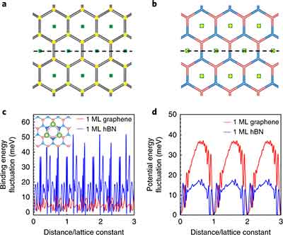 When graphene is placed on a crystalline substrate, the atomic potential of the wafer can influence the film grown above it. This makes it possible to form single-crystalline films while still keeping a weak interface for layer release.
Remote Epitaxy Through Graphene
Graphene is important in remote epitaxy because it is extremely thin, chemically stable, and can act as a release layer. A graphene-coated wafer may support epitaxial film growth and allow the finished film to be peeled away or transferred to another substrate.
Researchers use graphene-assisted remote epitaxy to explore reusable wafers, flexible films, and heterogeneous integration. This is especially useful when working with costly compound semiconductor substrates such as gallium arsenide wafers, GaN wafers, and other single-crystal materials.
Materials Used for Remote Epitaxy
Remote epitaxy can involve several wafer and thin-film materials depending on the device application. Common materials include:
- Graphene: Used as an ultrathin intermediate layer for epitaxial growth and film release.
- Silicon wafers: Used in semiconductor research, device development, and substrate comparison studies.
- Gallium arsenide wafers: Used for optoelectronics, high-frequency devices, and compound semiconductor films.
- GaN templates: Used for gallium nitride film growth, LEDs, power electronics, and RF device research.
- Silicon carbide wafers: Used for epitaxial graphene, high-power electronics, and high-temperature devices.
- Germanium wafers: Used in semiconductor, infrared, and advanced device research.
Benefits of Remote Epitaxy
Remote epitaxy is attractive because it may allow researchers to grow high-quality films while reducing material waste and substrate cost. The ability to separate the grown film from the wafer also supports flexible, transferable, and stacked device structures.
- Supports reusable wafer research
- May reduce the cost of compound semiconductor film production
- Allows thin films to be released and transferred
- Can help fabricate flexible and wearable electronics
- Supports heterogeneous integration of different semiconductor materials
- Useful for photonics, sensors, solar cells, LEDs, and advanced electronics
Applications for Remote Epitaxy
Remote epitaxy is being explored for a wide range of advanced semiconductor and electronics applications. Because it can support thin, flexible, and transferable films, it is especially useful for research involving materials that are difficult or expensive to grow using traditional epitaxy.
- Flexible electronics: Thin semiconductor films for bendable and wearable devices.
- Medical devices: Biocompatible and flexible electronic films for sensors and implantable device research.
- Photonics: Compound semiconductor films for optical and optoelectronic devices.
- Solar cells: Thin-film materials for photovoltaic and energy-harvesting devices.
- RF and power devices: GaN, GaAs, and SiC-based materials for high-frequency and high-power electronics.
- Heterogeneous integration: Stacking different crystalline materials into multifunctional devices.
Epitaxial Graphene and Remote Epitaxy
Epitaxial graphene is graphene grown on a crystalline substrate, commonly silicon carbide. It is studied for semiconductor, sensor, and electronic applications because of its electrical, thermal, and structural properties.
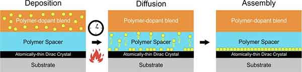 In remote epitaxy research, graphene can act as both a growth interface and a release layer. This makes it useful for creating thin semiconductor films that can later be transferred to flexible, transparent, or foreign substrates.
UniversityWafer, Inc. supplies graphene materials, silicon wafers, gallium arsenide wafers, GaN templates, and other substrates used in remote epitaxy and advanced semiconductor research.
Video: Defining Epitaxial Graphene