
Need some Si wafers for thin film passive circuits (conductor only). Our circuits are 41x28mm, so a wafer of between 4-6 inches would be best. We need 100 orientation, and the highest resistivity we can afford.
Wafers Used to Fabricate Passive Devices
A senior sensor architect requested the following quote:
Reference #213187 for specs and pricing.
Get Your Quote FAST! Or, Buy Online and Start Researching Today!
Related Photonics and Optical Substrate Resources
- Silicon wafers for photonics and waveguides
- SOI wafers for photonic integrated circuits
- Glass wafers for optical and photonics applications
- III-V semiconductor substrates for photonics
- Lithium niobate wafers for electro-optic devices
- Silicon nitride wafers for low-loss waveguides
- Sapphire wafers for photonics applications
- Photolithography for photonic device fabrication
Understanding The Importance Of Substrates In Fabricating Photonics Passive Circuits
Photonics, the science and technology of generating, controlling, and detecting light, has revolutionized various fields including telecommunications, data communication, sensing, and imaging. Within this domain, passive circuits play a crucial role in guiding and manipulating light for efficient signal processing and transmission. The success of these circuits heavily relies on the choice of substrates used during fabrication. Substrates serve as the foundation upon which photonics passive circuits are built.
They provide mechanical support while also offering essential electrical and thermal properties necessary for optimal circuit performance. The selection of substrates is critical as it directly impacts various circuit characteristics such as signal loss, propagation speed, thermal stability, and integration compatibility.
One key consideration when choosing substrates is their refractive index. This property affects how light interacts with the circuit components such as waveguides or resonators.
Additionally, other factors like transparency across a broad range of wavelengths and low optical absorption are crucial to minimize signal degradation. Moreover, mechanical properties like dimensional stability and compatibility with fabrication techniques become significant when ensuring long-term reliability of photonics circuits. Furthermore, thermal management is vital to prevent temperature-induced changes in circuit performance.

Exploring Common Substrates Used In Silicon Photonics: Silicon-On-Insulator Soi And Glass Substrates
Silicon photonics has emerged as a promising technology for the development of high-performance, low-cost photonic integrated circuits. One crucial aspect of fabricating photonics passive circuits is the choice of substrate material. This subtopic focuses on two commonly used substrates in silicon photonics: silicon-on-insulator (SOI) and glass substrates. Silicon-on-insulator (SOI) is a widely adopted substrate due to its excellent optical and electrical properties.
SOI consists of a thin layer of silicon device layer on top of an insulating buried oxide layer. This configuration allows for efficient light confinement and low propagation losses, making SOI an ideal platform for high-speed optical devices such as modulators, detectors, and waveguides. Additionally, its compatibility with complementary metal-oxide-semiconductor (CMOS) fabrication processes enables seamless integration with electronic components. Glass substrates also offer several advantages in silicon photonics applications.
Glass materials like silica provide a low-cost alternative to SOI substrates while still offering good transparency in the near-infrared wavelength range commonly used in telecommunications.
Leveraging Iii-V Semiconductor Substrates For Enhanced Performance In Photonics Passive Circuits
Photonics passive circuits play a crucial role in various technological advancements, ranging from telecommunications to sensing applications. These circuits consist of waveguides, filters, couplers, and other components that manipulate light for efficient signal transmission and processing. To fabricate such circuits, the choice of substrate material is paramount as it directly affects their performance characteristics. In recent years, III-V semiconductor substrates have emerged as a promising platform for enhancing the performance of photonics passive circuits.
III-V semiconductors are compound materials composed of elements from both group III and group V in the periodic table. The unique properties of these substrates offer several advantages over traditional materials like silicon. One significant advantage is their direct bandgap property, which enables efficient light emission and absorption at specific wavelengths. This property makes III-V semiconductor substrates particularly suitable for applications requiring precise control over light sources or detectors integrated within passive circuits.
Additionally, III-V semiconductors exhibit excellent carrier mobility and high electron saturation velocity compared to silicon-based substrates. This characteristic results in faster response times and lower signal losses in photonics passive circuits.
Alternative Substrates For Specific Applications: Lithium Niobate And Silica-Based Substrates
In the domain of photonics, where passive circuits play a vital role in enabling efficient light manipulation and transmission, selecting the right substrate material is crucial. While conventional substrates like silicon have been widely used, alternative materials are gaining attention for their unique properties and specific applications. Two such alternatives that have shown promise are lithium niobate (LiNbO3) and silica-based substrates.
Lithium niobate has emerged as a popular choice for various photonic devices due to its excellent electro-optic properties. Its high electro-optic coefficient allows for efficient modulation of light signals, making it ideal for applications such as modulators, switches, and frequency converters. Additionally, lithium niobate exhibits low optical loss and high thermal stability, further enhancing its suitability for photonics passive circuit fabrication.
Silica-based substrates offer exceptional performance in terms of low optical loss, high transparency across a broad wavelength range, and excellent thermal stability. These characteristics make them particularly well-suited for applications that require precise control over light propagation, such as waveguides and optical fibers. Silica-based substrates also exhibit compatibility with existing silicon-based fabrication processes, facilitating integration with other components in complex photonic systems.
Fabrication Techniques: Photolithography And Its Role In Creating High-Quality Photonics Passive Circuits
Photolithography is a fundamental fabrication technique widely used in the creation of high-quality photonics passive circuits. It plays a crucial role in defining the intricate patterns and structures required for various optical components, such as waveguides, filters, and splitters. The process begins with a substrate, typically made of materials like silicon dioxide or silicon nitride, which acts as the foundation for the circuit.
A thin layer of photoresist material is then coated onto the substrate surface. This photoresist layer is sensitive to ultraviolet (UV) light and can undergo chemical changes when exposed to it. Using a mask aligner or a stepper system, UV light is selectively projected onto the photoresist-coated substrate. The mask contains predefined patterns that determine the desired circuit layout. The areas exposed to UV light undergo either polymerization or degradation based on positive or negative resist types.
After exposure, the photoresist is developed using suitable chemicals, removing either the polymerized or degraded regions. This step transfers the pattern from the mask onto the substrate surface by creating openings for subsequent processing steps. Subsequent fabrication processes include etching or deposition techniques to create waveguides or functional layers within these openings.
What Substrates Use to Fabricate Photonics Passive Circuits
A printed circuit containing a resistor, inductor and capacitor has been fabricated on flexible PET substrates. The passive components were screen-printed using an Asys ASP01M screen printer with stainless steel screens.
Integrated photonics enable light to perform tasks that electronics have traditionally handled—from data transmission (5G networks) to precise metrology (like LiDAR in autonomous cars). These functions are typically implemented on silicon or indium phosphide PICs utilizing automated wafer-scale generic integration technology.
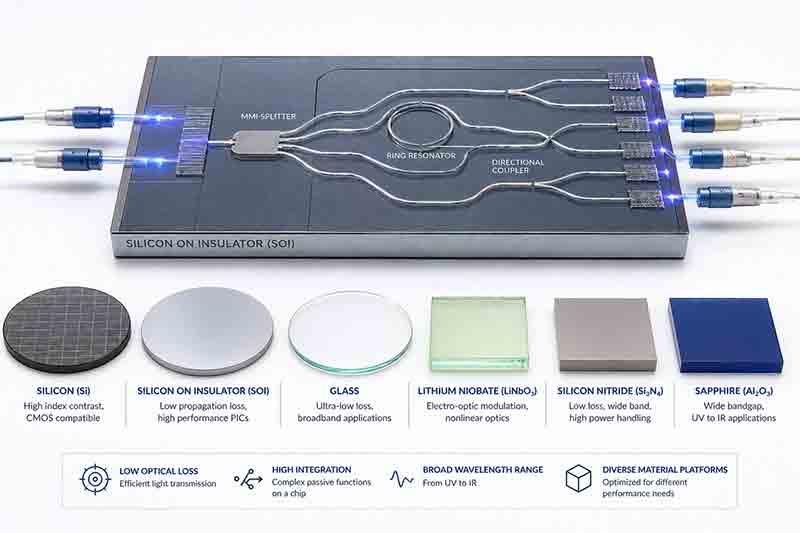
Fabrication of photonics passive circuits entails the use of various types of substrates. These substrates are often chosen based on the required optical properties, including refractive index, transparency, and compatibility with fabrication techniques. Some common substrates used in the fabrication of photonics passive circuits include:
-
Silicon (Si): Due to its high refractive index, silicon is an ideal substrate for waveguide-based devices. Silicon is also compatible with complementary metal-oxide-semiconductor (CMOS) fabrication technology, allowing for large-scale, low-cost production.
-
Silicon-on-Insulator (SOI): SOI substrates consist of a thin silicon layer on top of an insulating layer (usually silicon dioxide), which is then on top of a silicon wafer. This structure helps to confine light in the thin silicon layer, reducing propagation losses and improving device performance.
-
Silica (SiO2) or Glass: Used frequently for its excellent transparency properties in the visible and near-infrared ranges. Silica is often used for fiber optics and planar lightwave circuits.
-
III-V Semiconductors (e.g., Gallium Arsenide (GaAs), Indium Phosphide (InP)): These materials are often used for devices that require active functionalities like light emission or amplification because they can be doped to create direct bandgap materials. However, they are also used in some passive photonic circuits.
-
Lithium Niobate (LiNbO3): This crystal substrate is frequently used for modulators and other electro-optic devices due to its high electro-optic coefficient.
-
Silicon Nitride (Si3N4): Silicon nitride is known for its low optical loss and is often used for applications that require low-loss waveguides or high Q resonators.
-
Polymer substrates: Polymers can be engineered to have a wide range of optical properties, and their flexibility makes them suitable for certain applications like flexible optical interconnects. They are also compatible with low-cost fabrication methods.
-
Sapphire (Al2O3): This is a hard and robust substrate which exhibits low light scattering, making it suitable for applications that demand durability.
-
Chalcogenide Glasses: These are glasses based on sulfur, selenium or tellurium that have unique properties such as high nonlinear refractive index and high transparency in the infrared range.
Choosing a substrate depends on the specific requirements of the photonic passive circuit being fabricated. The desired performance, cost, integration density, and compatibility with other components all play a role in the selection process.