
"I am looking for 100 mm high-resistivity silicon wafers with carrier lifetimes greater than 100 μs. The wafers should preferably be Float Zone, undoped or lightly n-type, <100> orientation, and double-side polished. They will undergo front-side and back-side DRIE to fabricate micromachined waveguides excited by a laser."
Learn About Silicon Wafers & Semiconductor Technology
Whether you're new to semiconductor engineering or an experienced researcher, understanding silicon wafers, crystal growth, semiconductor fabrication, MEMS, photonics, and integrated circuit manufacturing is essential. UniversityWafer provides educational resources, recommended videos, and technical guidance to help students, engineers, and scientists better understand silicon materials and semiconductor processing.
Get Your Silicon Wafer Quote FAST! Or, Buy Online and Start Researching Today!
Recommended Videos to Learn About Silicon & Semiconductors
The following educational videos provide an excellent introduction to silicon wafers, semiconductor manufacturing, crystal growth, integrated circuits, photolithography, MEMS, and modern microelectronics. They are useful for students, researchers, educators, and engineers looking to expand their understanding of semiconductor technology.
Float Zone Silicon Wafers for Micromachined Waveguides
High-resistivity Float Zone (FZ) silicon wafers are frequently selected for micromachined waveguides, terahertz devices, photonics, and laser-based research because of their exceptional purity, long carrier lifetime, and low defect density.
Research Client Request:
UniversityWafer Recommended:
- 100 mm Diameter
- Undoped Silicon
- <100> Orientation
- >10,000 Ω-cm Resistivity
- 525 μm Thickness
- Double-Side Polished (DSP)
- Prime Grade
- TTV <10 μm
- Bow/Warp <30 μm
This wafer is widely used for deep reactive ion etching (DRIE), photonics, optical waveguides, terahertz research, MEMS fabrication, and other applications requiring long carrier lifetimes and ultra-high-purity silicon.
How Carbon Affects Monocrystalline Silicon
Carbon is one of several impurities that can be present during monocrystalline silicon crystal growth. Although carbon concentrations are typically very low, they can influence defect formation, oxygen interactions, and the mechanical properties of the crystal.
In Czochralski (CZ) silicon, carbon and oxygen are the two most common impurities introduced during crystal growth. Their concentrations and interactions affect crystal quality, thermal processing behavior, and device performance.
Rather than dramatically changing silicon's melting temperature, carbon primarily influences crystal defects, impurity precipitation, and dislocation formation during semiconductor manufacturing. Careful control of carbon concentration is therefore important when producing high-performance silicon wafers for integrated circuits, MEMS, power devices, and photonic applications.
Learn About Silicon & Semiconductor Technology
Whether you are new to semiconductor engineering or an experienced researcher, understanding silicon materials, wafer fabrication, crystal growth, and device physics is essential. The following books are widely recognized references used by universities, research laboratories, and semiconductor manufacturers around the world.
Recommended Semiconductor Books
Silicon Wafer Bonding Technology for VLSI and MEMS Applications
Editors: S. S. Iyer & A. J. Auberton-Hervé
This reference explains silicon wafer bonding techniques used in MEMS, VLSI, SOI wafer fabrication, and advanced semiconductor packaging. Topics include thermal treatment, stress reduction, oxide growth, and bonded wafer reliability.
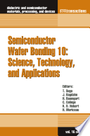
Semiconductor Manufacturing Technology
Authors: Michael Quirk & Julian Serda
A comprehensive introduction to semiconductor manufacturing covering wafer fabrication, cleanroom processes, lithography, oxidation, deposition, etching, diffusion, ion implantation, and semiconductor production equipment.
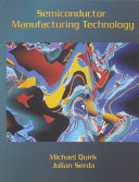
Semiconductor Device Fundamentals
Author: Robert F. Pierret
An excellent textbook introducing semiconductor physics, PN junctions, carrier transport, MOS devices, bipolar transistors, and integrated circuit fundamentals.

Physics of Semiconductor Devices
This classic reference covers quantum mechanics, carrier transport, tunneling, semiconductor device modeling, and practical applications used throughout the electronics industry.
Fundamentals of Power Semiconductor Devices
Author: B. Jayant Baliga
A leading reference explaining the operation and design of power MOSFETs, IGBTs, thyristors, Schottky diodes, and other high-power semiconductor devices.
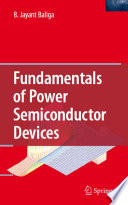
Semiconductor Manufacturing Handbook
Author: Hwaiyu Geng
A practical handbook covering semiconductor process integration, MEMS fabrication, yield improvement, packaging, sensors, and manufacturing best practices.
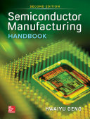
Fundamentals of Semiconductors
Authors: Peter Yu & Manuel Cardona
One of the most respected texts covering semiconductor materials, electronic properties, optical behavior, crystal structures, and carrier transport.

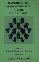
Handbook of Semiconductor Silicon Technology
Authors: William O'Mara, Robert Herring & Lee Philip Hunt
A comprehensive reference dedicated specifically to silicon crystal growth, wafer processing, defect reduction, contamination control, materials handling, and semiconductor manufacturing.
Can Silicon Be Doped with Compound Semiconductors?
A researcher asked whether silicon can be doped using compound semiconductors such as SnS, SnSe, GaP, or GaAs.
Research Question:
Can silicon or other substrates be uniformly doped with binary semiconductor materials, and what advantages would this provide?
UniversityWafer Response:
Bulk semiconductor crystals are manufactured with the goal of achieving the most uniform dopant distribution possible throughout the crystal. During crystal growth, manufacturers carefully monitor both radial and axial dopant uniformity to ensure consistent electrical performance.
Czochralski (CZ) silicon generally exhibits predictable axial dopant variation, while Float Zone (FZ) silicon provides exceptionally high purity and extremely uniform dopant concentrations. Neutron Transmutation Doping (NTD) offers another method for achieving highly uniform dopant distribution.
Most semiconductor devices, however, obtain their functional doping through diffusion or ion implantation after wafer fabrication, producing controlled dopant profiles near the wafer surface rather than throughout the entire substrate.
While compound semiconductors such as GaP, GaAs, and InP are commonly doped with multiple elements, intentional bulk silicon doping using III-V or II-VI compound semiconductors remains uncommon in commercial semiconductor manufacturing.
Related Silicon & Semiconductor Resources
- Silicon Wafers
- Silicon Wafer Applications
- Czochralski (CZ) Silicon Growth
- Float Zone (FZ) Silicon Wafers
- Undoped Silicon Wafers
- Doped Semiconductors
- Silicon-on-Insulator (SOI) Wafers
- Silicon Epitaxial Wafers
- Deep Reactive Ion Etching (DRIE)
- MEMS Substrates
- Photolithography
- Carrier Concentration
- N-Type Silicon Wafers
- P-Type Silicon Wafers
- Semiconductor Manufacturing