
We need high-resistivity float zone silicon (HRFZ Si) with 50.8 mm diameter and 3 mm thickness for terahertz beamsplitters.
Substrates for Terahertz Beamsplitters and THz Devices
UniversityWafer, Inc. supplies high-resistivity silicon, silicon-on-sapphire, gallium phosphide, ZnTe crystals, and quartz substrates for terahertz beamsplitters, electro-optical sampling, THz-TDS spectroscopy, and terahertz detection. Our materials support research in quantum nano-optoelectronics, photonics, and high-frequency electronics.
Float Zone Silicon for Terahertz Beamsplitters
A Quantum Nano-Optoelectronics researcher requested the following:
UniversityWafer, Inc. Quoted:
- 3-inch Float Zone Silicon wafer
- Resistivity >10,000 Ω-cm
- 76.2 mm diameter
- 3 mm thickness
- Double-side polished
- Quantity: 25 pieces
Reference #269299 for specifications and pricing.
Get Your Quote FAST! Or, Buy Online and Start Researching Today!
Silicon-on-Sapphire for THz Modulation
Researchers studying deep terahertz modulation requested silicon-on-sapphire (SoS) wafers to investigate photoexcitation and modulation of THz radiation using thin silicon films.
Reference #ONL29063 for specifications and pricing.
Gallium Phosphide for Terahertz Detection
Gallium phosphide (GaP) crystals are widely used for terahertz detection and electro-optical sampling due to their excellent optical and nonlinear properties.
A postdoctoral researcher requested:
- Undoped GaP (110)
- 10 × 10 × 0.5 mm, DSP
- 5 × 5 × 0.2 mm, DSP
Reference #255350 for pricing and availability.
Silicon Windows for THz-TDS Spectroscopy
A nanotechnology researcher requested high-resistivity silicon windows for time-domain spectroscopy (THz-TDS) over the 200 GHz to 5 THz range.
UniversityWafer supplied:
- 201 mm × 65 mm × 1.6 mm, DSP, >10K Ω-cm
- 201 mm × 65 mm × 3.1 mm, DSP, >10K Ω-cm
- 201 mm × 65 mm × 3.8 mm, DSP, >10K Ω-cm
All windows featured precision parallelism and beveled edges.
Reference #258947 for specifications and pricing.
ZnTe Crystals for Electro-Optical Sampling
Zinc Telluride (ZnTe) and GaP crystals are commonly used for terahertz electro-optical sampling.
A PhD candidate requested ZnTe (110) crystals and GaP (110) substrates with thicknesses near 0.5 mm for THz measurements.
UniversityWafer, Inc. Quoted:
- GaP (110), 5 × 5 × 0.5 mm, DSP
- ZnTe (110), 5 mm × 0.5 mm
- ZnTe (110), 10 mm × 0.5 mm
- Shipment: 6–7 weeks ARO
Reference #270778 for more information.
Double-Side Polished GaP for THz Detection
A graduate student studying terahertz detection requested:
Reference #274896 for pricing and lead time.
High-Resistivity Silicon for Terahertz Circuits
A PhD researcher studying terahertz and photonics passive circuits requested information on 8-inch high-resistivity silicon wafers with resistivities above 1 kΩ-cm. High-resistivity float-zone silicon (HRFZ Si) is widely used in THz devices because of its extremely low loss and excellent transmission characteristics.
UniversityWafer, Inc. quoted:
Item #3328
100 mm Undoped <100> Silicon
>20,000 Ω-cm resistivity
525 µm thickness
Single-side polished, prime grade
Reference #263806
What Materials Are Used for Terahertz Circuits?
Terahertz (THz) circuits operate in the frequency range between microwaves and infrared light. These devices are used in spectroscopy, imaging, wireless communications, sensors, radar systems, and quantum photonics. Material selection is critical because substrate losses directly affect device performance.
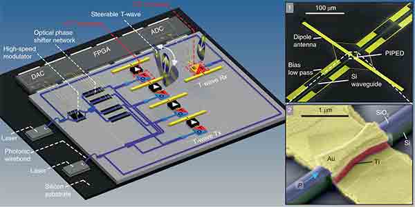
Terahertz Circuit Structure
Silicon Substrates for THz Applications
Silicon wafers remain one of the most commonly used materials for terahertz circuits. High-resistivity float-zone silicon offers low dielectric loss, excellent uniformity, and compatibility with semiconductor processing technologies.
Applications include:
- THz waveguides
- Photoconductive antennas
- THz modulators
- Spectroscopy systems
- Passive photonic circuits
- High-speed communication devices
Gallium Arsenide (GaAs) for Terahertz Devices
Gallium arsenide (GaAs) provides higher electron mobility than silicon and is commonly used for high-frequency devices, photoconductive switches, and THz emitters. GaAs substrates are widely employed in telecommunications, solar cells, microwave electronics, and terahertz directional couplers.
Its fast carrier response makes GaAs particularly attractive for ultrafast photonics and THz generation systems.
Indium Phosphide (InP) for High-Speed THz Electronics
Indium phosphide (InP) is another III-V semiconductor frequently used in terahertz transistors, photodetectors, and high-speed optoelectronic devices. InP offers superior electron velocity and excellent performance at very high frequencies.
InP substrates are commonly used to fabricate:
- Laser diodes
- Photodetectors
- Resonant tunneling diodes
- THz integrated circuits
- High-speed communication components
Silicon-on-Insulator (SOI) for THz Circuits
Silicon-on-insulator (SOI) substrates improve performance at terahertz frequencies by reducing parasitic capacitance and electrical losses. SOI technology is widely used for RF devices, millimeter-wave electronics, and integrated THz components.
The insulating oxide layer helps achieve better signal integrity and higher operating frequencies compared with conventional silicon.
Fused Quartz Windows for Terahertz Measurements
Fused quartz and fused silica windows exhibit excellent transparency throughout the terahertz spectrum. Their low thermal expansion, high chemical purity, and low dielectric loss make them ideal for THz spectroscopy, waveguides, vacuum windows, and optical systems.
Researchers often request quartz windows with diameters around 50 mm and thicknesses ranging from 0.5 mm to 2 mm for frequencies between 0.1 and 3 THz.
Thin Quartz Wafers for THz Wave Applications
Ultra-thin quartz wafers are increasingly used for specialized terahertz wave experiments. Double-side polished quartz with thicknesses below 50 µm can be fabricated for structural dynamics studies and advanced THz devices.
UniversityWafer supplied:
- Single crystal quartz wafer
- 1-inch diameter
- 45.7 µm thickness
- Double-side polished
- Quantity: 10 pieces
Reference #272647 for specifications and pricing.
Applications of Terahertz Circuits
Terahertz electronics are enabling breakthroughs in:
- Wireless communications
- THz spectroscopy
- Security imaging systems
- Biomedical diagnostics
- Radar technologies
- Quantum photonics
- High-speed sensors
- Integrated photonic circuits
- Material characterization
UniversityWafer, Inc. supplies high-resistivity silicon, quartz, gallium arsenide, indium phosphide, silicon-on-insulator, ZnTe, GaP, and other substrate materials for advanced terahertz research and production.
Related THz and Photonics Pages
- Silicon Wafers
- Silicon-on-Sapphire (SoS)
- Silicon-on-Insulator (SOI)
- Single Crystal Quartz Wafers
- Fused Silica Windows
- Gallium Phosphide (GaP) Wafers
- Gallium Arsenide (GaAs) Wafers
- Indium Phosphide (InP) Wafers
- ZnTe Crystals
- Integrated Photonics
- Photonic Passive Circuits
- RF Device Applications
- HEMT Structures
- Interposer Technology
- Materials Science Applications